When I look inside a chip from the popular 7400 series, I know what to expect: a fairly simple die, implemented in a straightforward, cost-effective way. However, when I looked inside a military-grade chip built by Integrated Device Technology (IDT)4 I found a very unexpected layout: over 1500 transistors in an orderly matrix. Even stranger, most of the die is wasted: less than 20% of these transistors are used, forming scattered circuits connected by thin metal wires.
In this blog post, I look at this chip in detail, describe its gates, and explain how it implements the "1-of-4" decoder function. I also discuss why it sometimes makes sense to build chips with a gate array design such as this, despite the inefficiency.
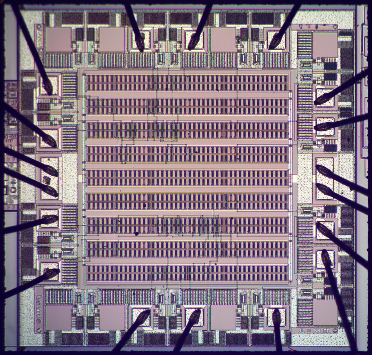
In the photo below, you can see the silicon die in more detail, with the silicon appearing pink. The main circuitry is implemented in the nine rows that form the gate array, a grid of 1584 transistors. The tiny dark rectangles are transistors of two types, NMOS and PMOS, that work together to implement CMOS logic circuits. At this scale, the metal wiring is visible as faint gray lines and smudges, but most of the transistors are unconnected. Surrounding the gate array are 22 input/output (I/O) blocks each with a square bond pad. As with the transistors, many of these I/O blocks are unused. Fourteen of these bond pads have tiny metal bond wires (the thick black lines) that connect the silicon die to the chip's external pins. Finally, the pairs of bond wires at the center left and center right provide ground and power connections for the chip.
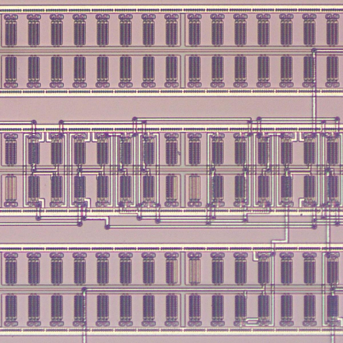
The photo below zooms in on three rows of circuitry in the chip. The large dark rectangles are pairs of transistors, with two lines of transistors in each row of circuitry. At the top and bottom of each row, the thick horizontal white lines are metal wiring that provides power and ground. In each row, one line of transistors holds PMOS transistors, next to the power wiring, while the other line holds NMOS transistors, next to the ground wiring. (The orientation flips in each successive row, so it isn't obvious which transistors are which unless you check the power connections at the end of the row.)
The transistors are wired into gates by the metal layers, the white lines. The gates are connected by horizontal and vertical wiring using the wiring channels between the rows. This wiring style is very similar to standard-cell logic. However, unlike standard-cell logic, the underlying transistor grid is fixed, resulting in wasted transistors. In the image above, most of the transistors in the middle row are used, while the top row is unused and the bottom row is mostly unused.
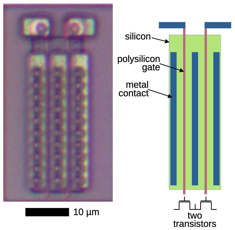
The diagram below shows the structure of one of the transistor blocks, which contains two tall, thin MOS transistors. The vertical metal contacts connect to the sources and drains of the transistors, with the two transistors sharing the middle contact. (On an integrated circuit, the source and drain of a transistor are identical, so it is arbitrary which side is the source and which is the drain.) The short horizontal metal contacts at the top connect to the gates of the two transistors; the gates are made of polysilicon, which is barely visible in the die photo. The gates partition the active silicon (green), forming the transistors. The gate width is approximately 1 µm.
NAND gate
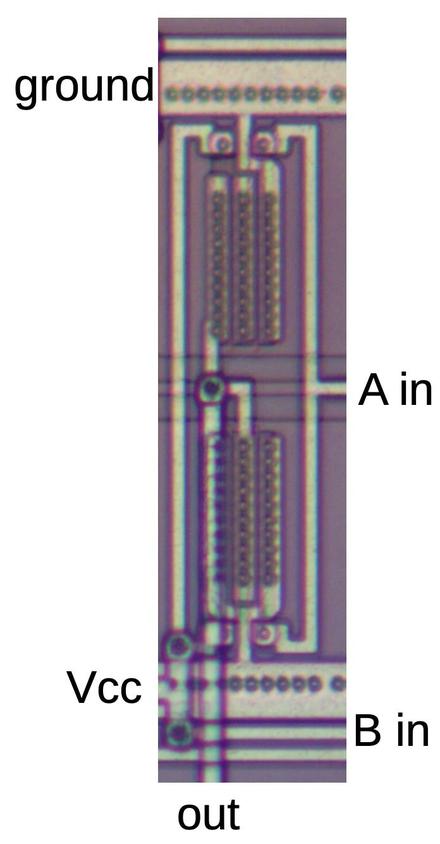
In this section, I'll explain the construction of one of the NAND gates on the die. The NAND gate below uses four transistors, two NMOS transistors on the top and two PMOS transistors on the bottom. The white lines are the metal wiring, forming two layers. Most of the wiring (including power and ground) is in the lower (M1) layer. The slightly wider and darker vertical segments are the upper (M2) layer. The circles connect the metal layers when they join, or connect the metal layer to the underlying silicon or polysilicon. With two metal layers, it's a bit tricky to see how the wiring is connected. The A and B inputs each connect to two transistor gates. The transistor group at the top is connected to ground on the right, with the output on the left. The transistor group on the bottom is connected to Vcc on the left and right, with the output in the middle. This has the effect of putting the upper transistors in series and the lower transistors in parallel.
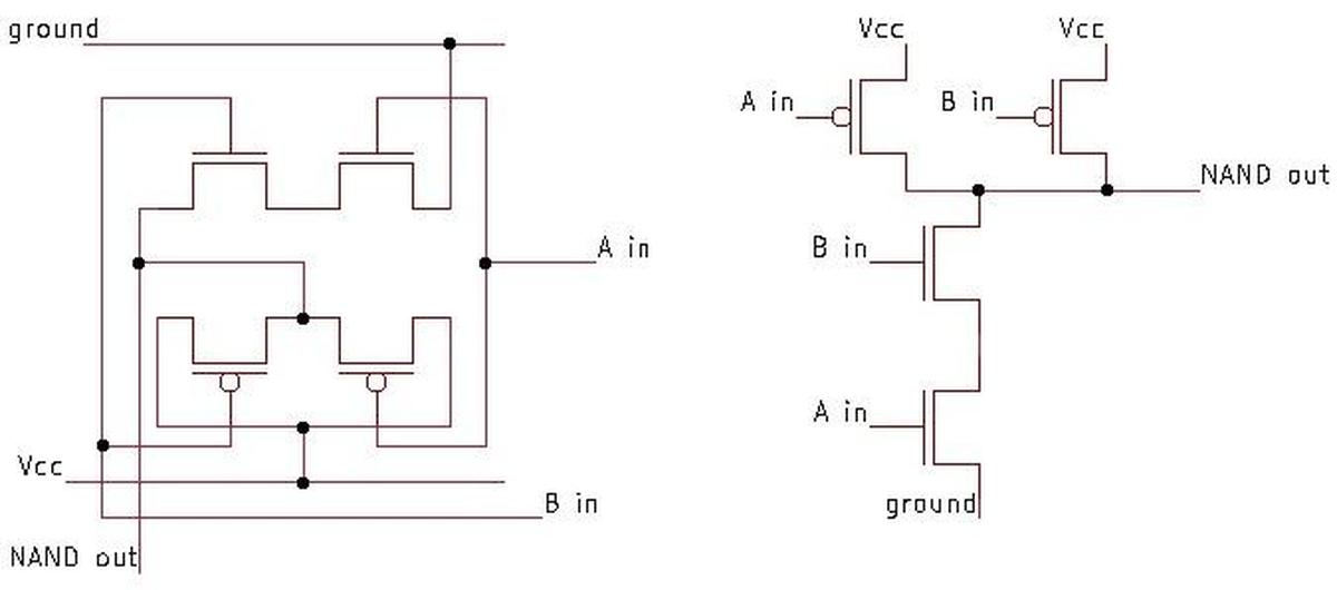
Below, I've drawn the schematic of the NAND gate. On the left, the layout of the schematic matches the die layout above. On the right, I've redrawn the schematic with a more traditional layout. To understand its operation, note that a PMOS transistor (top on the right schematic) turns on when the input is low, while an NMOS transistor (bottom on the right) turns on when the input is high. When both inputs are high, the two NMOS transistors turn on, connecting ground to the output, pulling it low. When either input is low, one of the PMOS transistors turns on, pulling the output high. Thus, the circuit implements the NAND function. The NMOS and PMOS transistors operate in a complementary fashion, giving CMOS (Complementary MOS) its name.
NOR gate
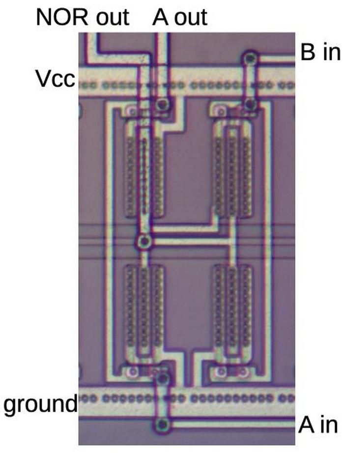
In this section, I'll explain the layout of one of the NOR gates on the die, shown below.
This gate is twice as large as the previous NAND gate so it can provide twice the output current.1
The NOR gate uses eight transistors, four PMOS transistors in the upper half and four NMOS transistors in the lower half.
(Note that Vcc and ground are flipped compared to the previous gate, as are the NMOS and PMOS transistors.)
The two transistors in each block are wired in parallel to produce more current for
the output.
(A out is the same signal as A in, exiting the block at the top to connect to other circuitry.)
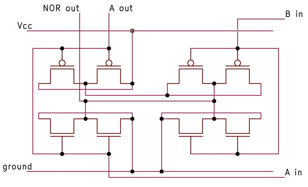
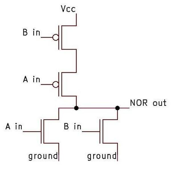
The schematic below shows the wiring of the eight transistors. The schematic layout corresponds to the physical layout to make it easier to map between the image and the schematic. The upper transistor groups are wired in series, while the lower transistor groups are wired in parallel.
The schematic below has been redrawn to make the functionality clearer, and the parallel transistors have been removed. If either input is high, one of the NMOS transistors on the bottom will turn on and pull the input low. If both inputs are low, the two PMOS transistors will turn on and pull the input high. This provides the desired NOR function.
Note that the NAND and NOR gates have similar but opposite schematics. In the NAND gate, the NMOS transistors are in series while the PMOS transistors are in parallel. In the NOR gate, the roles of the transistors are swapped.
The chip's circuit
The chip I examined is a "dual 1-of-4 decoder with enable".2 The decoding function takes a two-bit input and selects one of four output lines depending on the binary value. The enable line must be low to activate this operation; otherwise all four output lines are disabled. The chip contains two of these decoders, which is why it is called a dual decoder. In total, the chip contains 18 logic gates,3 so it is very simple, even by 1990s standards.
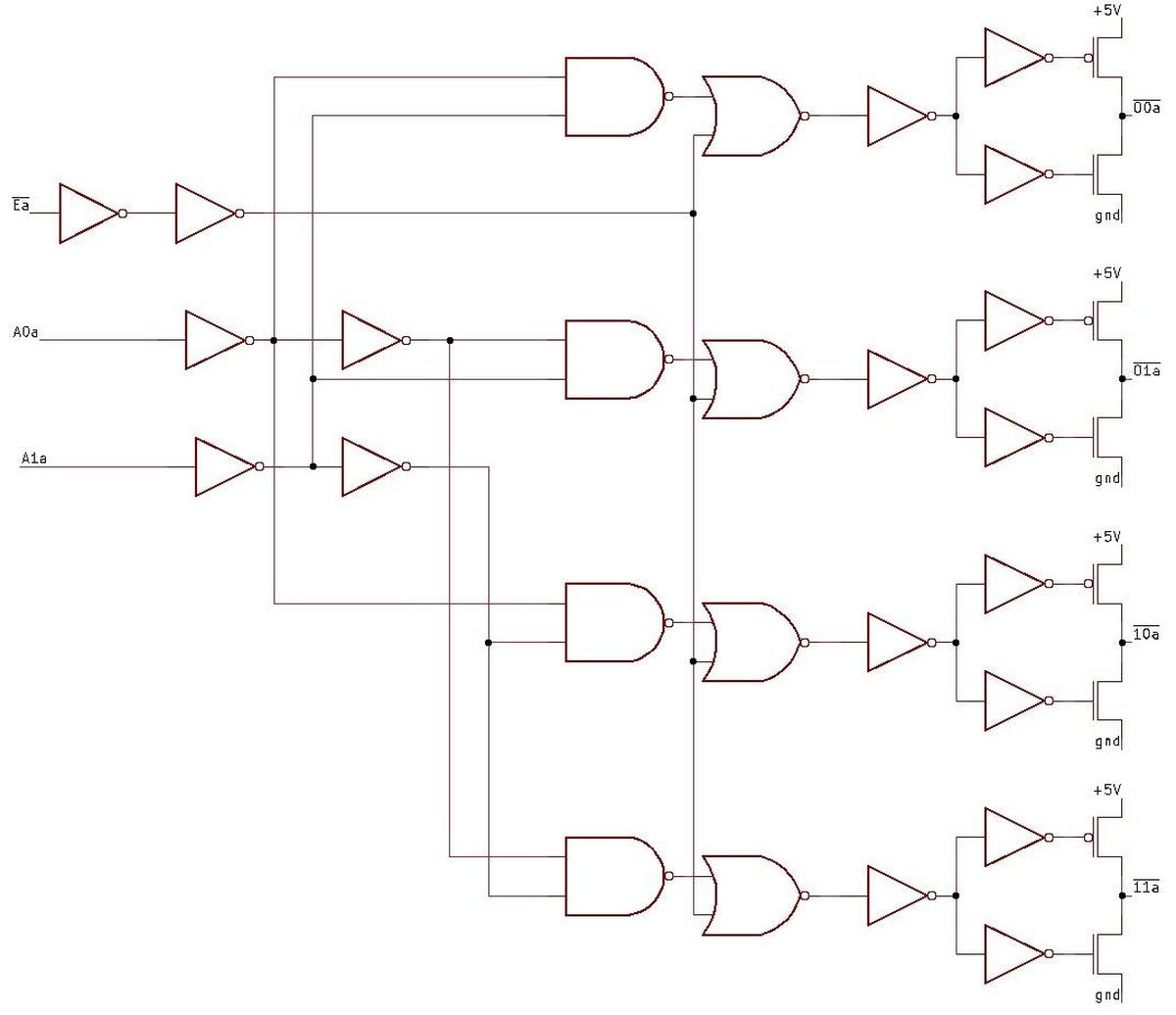
I reverse-engineered the chip and created the schematic below, showing one of the dual units.
Each NAND gate matches one of the four input possibilities to drive one of the four outputs.
The NOR gates support the ENABLE signal, blocking the outputs unless ENABLE is active (i.e. low).
The chip uses a general-purpose I/O block (below) for each pin, that can be used as an input or an output depending on how it is wired. Each block contains two large drive transistors: an NMOS transistor to pull the output low and a PMOS transistor to pull the output high. The I/O block has separate control lines for the two output transistors. (At the bottom of the image below, two thin metal wires drive the high-side and low-side transistors.) This permits tri-state logic: if neither transistor is energized, the output is left floating. The gate array drives the output transistors with high-current inverter, constructed from multiple transistors in parallel. (This is why the schematic shows more inverters than may seem necessary.)
When used as an input, the pad is wired to the surrounding circuitry slightly differently, connecting to input protection diodes (not shown on the schematic). Thus, the functionality of the I/O blocks can be changed by modifying the metal layers, without changing the underlying silicon.
Some 7400-series history
The earliest logic integrated circuits used resistors and transistors internally, so they were called RTL (Resistor Transistor Logic), but RTL had significant performance problems. RTL was rapidly replaced by Diode Transistor Logic (DTL) and then Transistor Transistor Logic (TTL). In 1964, Texas Instruments created a line of TTL integrated circuits for military applications called the SN5400 series. This was shortly followed by the commercial-grade SN7400 series.
The 7400 series of integrated circuits was inexpensive, fast, and easy to use. The line started with simple logic circuits such as four NAND gates on a chip, and moved into more complex chips such as counters, shift registers, and ALUs. The 7400 series became very popular in the 1970s and 1980s, used by electronics hobbyists and high-performance minicomputers alike. These chips became essential building blocks and "glue" logic for microcomputers, heavily used in the Apple II for instance.
The original 7400 series branched into dozens of families with different performance characteristics but the same functionality. The 74LS (low-power Schottky) family, for instance, became very popular as it both improved speed and reduced power consumption. In the mid-1970s, 7400-series chips were introduced that used CMOS circuitry instead of TTL for dramatically lower power consumption. This CMOS family, the 74C series, was followed by numerous other CMOS families.
That brings us to the chip I examined, a member of IDT's 74FCT (Fast CMOS TTL-compatible) line of chips, introduced in the mid-1980s. (Specifically, it is in the 54FCT family because it handles a wider temperature range.) These chips used advanced CMOS technology to provide high speed, low power consumption, and as a military option, radiation tolerance.
Conclusions
Why would you make a chip in this inefficient way, using a gate array that wastes most of the die area? The motivation is that most of the design cost can be shared across many different part types. Each step of integrated circuit processing requires an expensive mask for photolithography. With a gate array, all chip types use the same underlying silicon and transistors, with custom masks just for the two metal layers. In comparison, a fully custom chip might require eight custom masks, which costs much more. The tradeoff is that gate array chips are larger so the manufacturing cost is higher per device.5 Thus, a gate array design is better when selling chips in relatively small quantities, while a custom design is cheaper when mass-producing chips.6 IDT focused on the high-performance and military market rather than the commodity chip market, so gate arrays were a good fit.
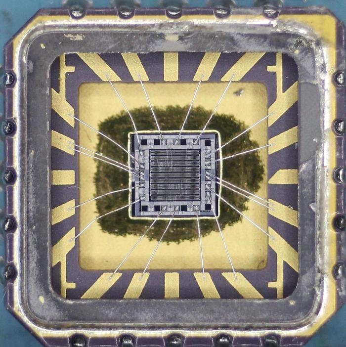
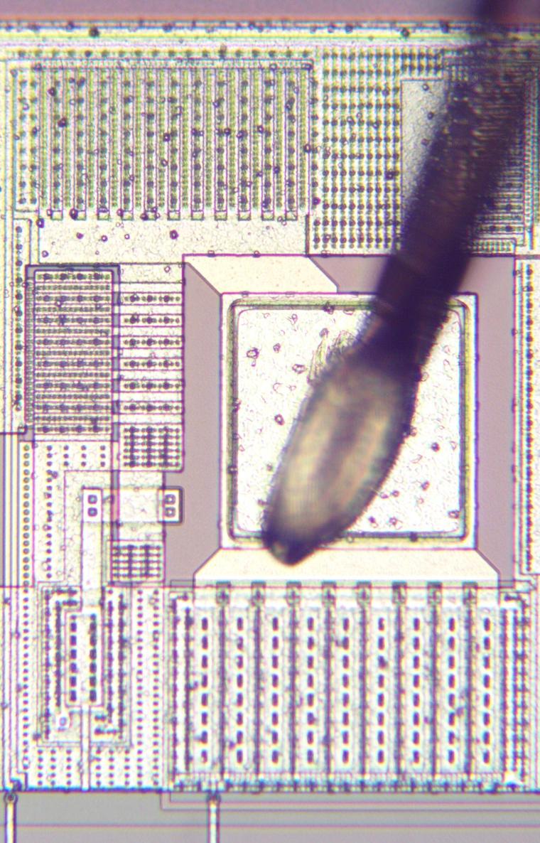
One last thing. The packaging of this chip is very interesting since it is mounted on a multi-chip module. The module also contains two Atmel EEPROMs. Presumably the decoder chip decodes address bits to select one of the EEPROMs.
Thanks to Don S. for providing the chip. Follow me on Twitter @kenshirriff or RSS for updates. I've also started experimenting with Mastodon recently as @oldbytes.space@kenshirriff.
Notes and references
-
Properly sizing the transistors in a gate is important for performance. Since the transistors in the gate array are all the same size, multiple transistors are used in parallel to get the desired current. The 1999 book Logical Effort describes a methodology for maximizing the performance of CMOS circuits by correctly sizing the transistors. ↩
-
The part number is "IDT 54FCT139ALB". "54" indicates the chip operates under an enhanced temperature range of -55°C to +125°C. The "A" indicates the chip is 35% faster than the base series (but not as fast as "C"). "L" indicates the chip is packaged in a leadless chip carrier, the square package shown at the top of the article. Finally, "B" indicates the chip was tested according to military standards: MIL-STD-883, Class B. ↩
-
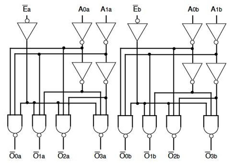
The chip contains 18 logic gates according to the functional schematic in the datasheet (below). The implementation actually uses 52 logic gates by my count (2×26) because the implementation doesn't exactly match the schematic. In particular, the datasheet shows three-input NAND gates, but the chip uses a NAND gate and a NOR gate along with inverters. The chip also has additional inverters to drive the output transistors in each I/O block.
Schematic of the chip from the datasheet. -
Integrated Device Technology was a spinoff from Hewlett Packard that started in 1980. IDT built advanced CMOS chips including fast static RAM and microprocessors (bit-slice and MIPS). It became part of Renesas in 2018. A very detailed 1986 profile of IDT is here. IDT's logo is pretty cool, combining a chip wafer and calculus.
The logo of Integrated Device Technology.Here's how the logo looks on the die:
Closeup of the die showing the IDT logo.The die also has the initials of the designers, along with some mysterious symbols. One looks like the Chinese character "正". (Update: based on a Twitter comment, these symbols are probably tally marks, indicating the revision count for each mask.)
Closeups of two parts of the die. -
Integrated circuit manufacturing is partitioned into the "front end of line", where the transistors are created on the silicon wafer, and the "back end of line", where the metal wiring is put on top to connect the transistors. With a gate array construction, the front end of line steps create generic gate array wafers. The back end of line steps then connect the transistors as desired for a particular component. The gate array wafers can be produced in large quantities and stored, and then customized for specific products in smaller quantities as needed. This reduces the time to supply a particular chip type since only the back end of line process needs to take place. ↩
-
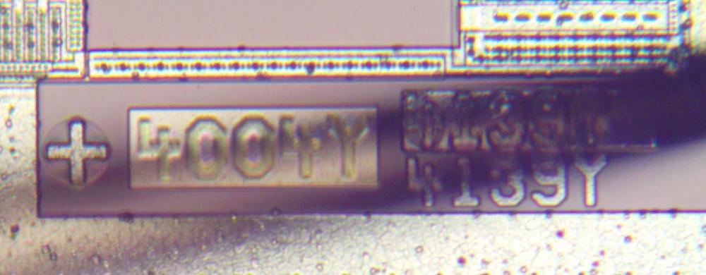
The IDT High-Speed CMOS Logic Design Guide briefly mentions the gate array design. The FCT family was built from two sizes of gate arrays, "4004" for smaller chips and "8000" for larger chips. Later, IDT shrunk the original "Z-step" gate arrays to smaller, higher-performance "Y-step" arrays. They then customized some of the devices to create the "W-step" devices. Looking at the markings on the die, we see that this chip uses the "4004Y" gate array.
The die shows gate slice 4004Y and part 4139Y (indicating 54139 or 74139). The numbers are slightly obscured by a bond wire.




13 comments:
"Reverse-engineered schematic of half the chip" has an error...
a dot
Thanks Steve, I've fixed the schematic.
A while back I had a related idea: UTTL (Universal TTL). Each IC contains the effective complete set of logic functions for a given pin count and is PROM programmable. You power it with a reverse current, which puts it in programming mode and then all but one of the other signals select the actual TTL function code and the remaining signal latches it. The function code is then used to blow the correct set of fuses and when the IC is powered properly, it has the expected, programmed TTL function.
The real advantage of UTTL is to compensate for the much smaller range of TTL circuits sold by most electronic outlets.
Ken, can you please ellaborate on how ENABLE works ? From my understanding, when ENABLE is low, all the outputs are strongly tied to +5V. Schematics does not show any way of controlling individual transistors in output drivers.
gtalk, the ENABLE is active-low. When it is high, it forces the NOR gates to output low, which turns on the PMOS pull-up transistors in the output drivers, pulling the outputs high.
Snial, you are kind of describing FPGAs or CPLDs. They read in a ROM to a long shift register, where every 3-4 bits control one gate cell, telling it what function that cell should perform.
I will venture to guess on the rationale for this chip design. First, these were inexpensive devices, so spreading the engineering costs over multiple products is a benefit. Many memory devices from that era included the capability to ship in different widths, like a 1-bit/4-bit combination.
Also, the bond pads are pretty close. A tiny chip would become bond pad limited, where the chip can't decrease below a certain size for a given bond pad configuration. I couldn't tell what the bond pad spacing is, maybe knowing this space would allow a packaging engineer to say if this chip was bond pad limited.
Hi Josh O,
Yes, I'm sort-of describing an FPGA or CPLD, but with a trivial, parallel, programming process - trivial enough for chips to be programmed easily with minimal and importantly, open tools, namely: in production, the ID of the intended target chip is directly latched. Consider two basic TTL chips:
7400: The pin order is: 1A, 1B, 1Y 2A, 2B, 2Y, GND, 3Y, 3B, 3A, 4Y, 4B, 4A, VCC.
7474: The pin order is: 1/CLR, 1D, 1Clk, 1/PRE, 1Q, 1/Q, GND, 2/Q, 2Q, 2/PRE, 2Clk, 2D, 2/CLR, VCC
These are fairly different. The point of programming by reversing the GND and VCC pins (a bridge rectifier handles this so that the normal operation of the device isn't powered, but the fuses are connected) is so that no pins are lost and the chip remains 100% compatible with either function.
So, then we have for both chips:
7400 and 7474: The programming pins are: Id0, Id1, Id2, Id3, Id4, Id5, VCC, Id8, Id9, Id10, Id11, R/W, CLK, GND.
Id<11:0> for the 7400 could be 0x00, and for the 7474 it could be 0x4A. We power the chip with CLK=1, set R/W=0, set Id<11:0> to the appropriate ID and clock CLK low then high. Then R/W is set high and CLK is repeatedly clocked until Id<11:0> returns a 'Programmed' identifier. Internally, the IC could easily be a small CPLD configured by a shift register, but one that's set up by latching the ID.
Although an FPGA or CPLD could perform the functionality of any one (and up to millions) of the 74 series ICs in a single packages by an appropriate serially downloaded ROM program, this is intended for situations where a hardware designer would actually use a traditional TTL chip, such as a latch or some minor glue logic, which happens surprisingly often.
And the key thing is that it simplifies BOMs, because the part numbers for all the 14-pin 74 series chips are now the same, instead there's a production step to assign the correct function.
Does that make sense?
The caption under the module photo incorrectly says "AT28HC64 EPROM" when they're EEPROMs as mentioned in the text
Dear Ken, I've read in the past your 6502 overflow explanation, that helped me understand flags and move forward in my TTL-based 6502 build.
It is now the first time I'm trying to understand what generally happens at the silicon level inside a chip; your explanation is great! I spotted a typo in this sentence:
The schematic below has been redrawn to make the functionality clearer, and the parallel transistors have been removed. If either input is high, one of the NMOS transistors on the bottom will turn on and pull the **input** OUTPUT low. If both inputs are low, the two PMOS transistors will turn on and pull the **input** OUTPUT high. This provides the desired NOR function.
I embedded the wrong words in ** and added the correct word in CAPS.
Regards,
Andrea / Italy
It's me again :-)
I understand gtalk2voip doubts: in these two sentences it seems that the chip is working like a tri-state, but actually it's not:
-- The enable line must be low to activate this operation; otherwise all four output lines are disabled.
-- The NOR gates support the ENABLE signal, blocking the outputs unless ENABLE is active (i.e. low).
Maybe it is a misunderstanding on my side because I'm not native English speaker?
Wouldn't it be better to say
-- The enable line must be low to activate this operation; otherwise all four output lines are forced high.
-- The NOR gates support the ENABLE signal, forcing the outputs high unless ENABLE is active (i.e. low).
Just asking, I don't want to teach you anything, I'm just trying to fully understand :-)
Andrea
@Snial A diode bridge, even a Schottky diode bridge, would limit the performance of the programmable chips. If you want to learn how programming could be done simply - read the Monolithic Memories Inc. databooks circa 1983. MMI made the original PAL (programmable array logic) chips. These chips did not have dedicated programming pins. The programming logic was activated by feeding voltages much higher than the rated 5V to certain pins, thus activating the programming circuits. Without the high voltage, the programming circuits were dormant. Furthermore, there was a "final" fuse that disabled readback and further programming, thus "finalizing" the chip's configuration. It certainly would have been possible to make universal TTL chips that way, as PALs were also bipolar logic chips. They'd need a fairly large die area, though, since the chips would need a ROM that defines every logic function. The simple programming operation that "selects" the chip would then most likely trigger internal programming circuit that transfers the contents of a selected slice of the ROM to the fuses. It would have been costly, but perhaps manufacturing it en-masse would make it affordable. These would still be relatively simple chips, and using a modern-ish CMOS process the dies could cost a couple cents each at most.
Post a Comment