The 6502 microprocessor chip
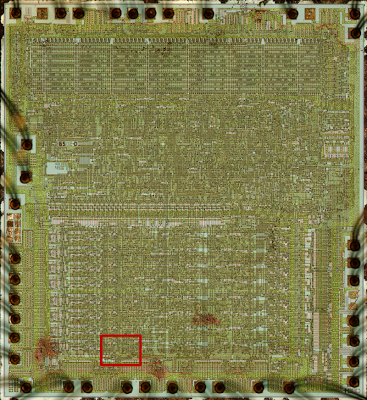
The 6502 is an 8-bit microprocessor that was very popular in the 1970s and 1980s, powering popular home computers such as the Apple II, Commodore PET, and Atari 400/800. The following photograph shows the die of a 6502 processor. Looking at the photograph, it seems impossibly complex, but it turns out that it actually can be understood, using the Visual 6502 group's reverse engineered 6502. The red box shows that part of the chip that will be explained in this article. The 6502 chip is made up of 4528 transistors (3510 enhancement transistors and 1018 depletion pullup transistors). (By comparison, a modern Xeon processor has over 2.5 billion transistors, which would be almost hopeless to try to understand.)
As a rough overview of the above photograph, the edge of the die shows the wires going to the pins. Approximately top fifth of the chip (with the regular rectangular pattern) is the PLA that decodes instructions. The middle third is a bunch of logic, mostly to do additional decoding of instructions. The bottom half has the registers, ALU (arithmetic-logic unit), and main busses. They are all 8 bits, with each bit in a horizontal layer. The high-order bit is at the bottom of the photo, and this is where the overflow logic lies.
The overflow formula
In brief, if an unsigned addition doesn't fit in a byte, the carry flag is set. But if a signed addition doesn't fit in a byte, the overflow flag is set. The 6502 processor computes the overflow bit for addition from the top bits of the two operands (A7 and B7), and the carry out of bit 6 into bit 7 (C6):
V = not (((A7 NOR B7) and C6) NOR ((A7 NAND B7) NOR C6))
For a more detailed explanation of what overflow means, see my previous article or The overflow flag explained.
Gate-level implementation
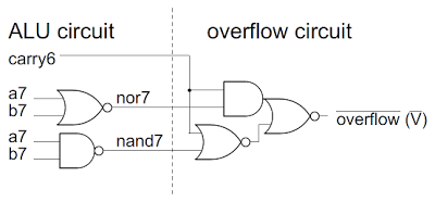
Described as gates, the actual circuit to generate the overflow flag in the 6502 turns out to be surprisingly simple. It uses the carry out of bit 6, and the top bits of the two arguments A and B. Since the values of NAND(a7, b7) and NOR(a7, b7) are already available in the ALU (Arithmetic-Logic Unit) for other purposes, the actual overflow circuit is simply the three gates on the right. (The ALU is, of course, much more complex than the part shown above.) This circuit can be seen at the bottom of the 6507 schematic (where the inverted overflow value is called FLOW). You might wonder why the circuit uses NAND and NOR gates so heavily; it turns out that these are much easier to implement with transistors than AND and OR gates.
Transistor-level implementation

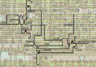
The circuit above shows the actual implementation of the overflow circuit in the 6502 using NMOS transistors. The circuit to generate the overflow flag is very simple, requiring just a few transistors to implement the three gates. A, B, and carry are the inputs, and the output #overflow indicates complement of the overflow signal.
MOS transistors are fairly easy to understand, since they operate like switches. Most of the transistors are NMOS enhancement mode transistors, which can be considered as switches that close if the gate has a positive input, and are open otherwise. The transistors with a black bar are NMOS depletion mode transistors, which can be considered as pull-up resistors, giving a positive output if nothing else pulls the output low.
The three transistors on the left implement a simple logic gate to compute NAND of A and B. If both inputs A and B are positive, the switches close and connect the output to ground (the horizontal line at the bottom). Otherwise, the pullup transistor connects the output to the positive voltage (circle at the top). Thus, the output is the NAND of A and B - 0 if both inputs are positive, and 1 otherwise.
The next three transistors compute NOR of A and B. If A, B, or both are positive, the associated transistor is switched on and connects the output to ground. Otherwise the output is positive.
The remaining transistors are the actual overflow circuit. The next group of three transistors is a NOR gate, which was described above. It computes the NOR of the carry and the NAND output from the ALU, feeding its output into the final group of four transistors. The four transistors on the right implement an AND gate and NOR gate in a single circuit. If the output from the previous circuit is 1, the rightmost transistor switches on, pulling the output (inverted V) to ground. If both NOR7 and CARRY6 are 1, the two associated transistors switch on, pulling the output to ground. Otherwise, the pullup transistor keeps the output high. The result is the complemented overflow value.
Going to the silicon
Now that you've seen how the circuit works at the transistor level, the silicon level can be explained.We'll begin with an (oversimplified) description of how the chip is constructed. The chip starts with the silicon wafer. Regions are diffused with an element such as boron, yielding conductive n+ diffusion regions. On top of the polysilicon layer is a layer of metal "wires" providing more connections. For our purposes, diffusion regions, polysilicon, and metal can all be consider conductors. In the 6502, the polysilicon connections run roughly vertical, and the metal wires run generally horizontal.
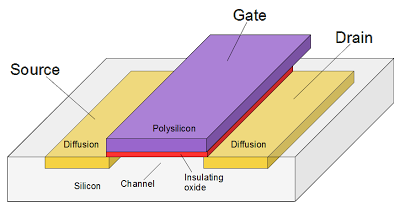
To build a transistor, two n+ regions are separated by an undiffused region. A thin insulating oxide layer on top forms the transistor gate, which is wired to a diffusion line. When charge is applied to the gate via the polysilicon line, the two n+ regions can conduct.
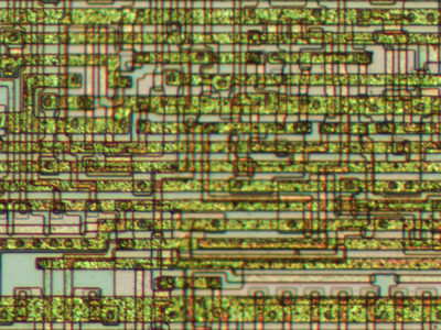
The follow picture zooms in on the base silicon layer in the 6502, showing the region in the red outline. The darker gray regions are n+ diffusion areas, which have been doped to be conducting. The white stripes that separate n+ regions are the transistor gates, showing the thin insulating oxide layer that switches on and off conduction between the neighboring n+ regions. The gray squares are vias, which connect to other layers.
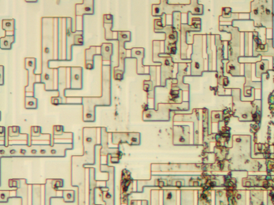
The next picture shows the polysilicon and metal layers that lie on top of the base silicon. This picture is aligned with the previous one, and you may be able to pick out some of the diffusion layer underneath. The whitish vertical stripes are conductive polysilicon. The greenish metallic-looking horizontal stripes are in fact metal, forming conductors. The gray square are vias, which connect different layers. Note that the chip is crammed full of conductors, making it hard at first glance to tell what is going on.
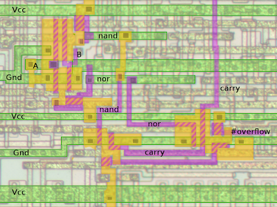
The final picture explains exactly what is happening at the silicon level. It labels the different layers that take part in the overflow circuit with different colors. The lowest layer is the diffusion layer in yellow. On top of this is the polysilicon layer in purple. The topmost layer of metal is in green. Power (Vcc) and ground are supplied through the metal layer. The crosshatches show transistor gates, formed by polysilicon over insulating oxide. The skinny crosshatched areas are the enhancement transistors used as switches. The blocky crosshatched areas connected to Vcc (positive voltage) are the depletion transistors used as pullups.
The circuit can be understood starting in the upper left. A and B are bit 7 of the A and B values going into the ALU. (A and B come from elsewhere in the processor.) If A and B are positive, the two upper transistors (vertical crosshatches) will pull the NAND output low. If A or B are positive, one of the two transistors below will pull the NOR output low. The NAND and NOR outputs travel to multiple parts of the ALU through metal, polysilicon, and diffusion "wires", but only the relevant connections are shown.
In the lower left is the first gate of the overflow circuit, computing the NOR of the NAND output and carry (which comes from elsewhere in the chip). The polysilicon line (purple) on the bottom is the output from this gate. In the lower right is the second gate of the overflow circuit, combining the NOR, carry, and output of the first gate. The result is #overflow (i.e. inverted overflow).
You can see this circuit in action in the Visual 6502 simulator. The color scheme in the simulator is different - diffusion is green, yellow, orange, and red. The metal layer is shown in ghosted white, but Vcc and ground are omitted. Polysilicon is in purple, and the transistors are not explicitly shown.
16 comments:
The 6502 was an absolutely awesome breakthrough by just a few engineers. It was the inspiration behind ARM.
Excellent walkthrough! Posted to http://forum.6502.org
Awesome article ! Brings back the memories few decades old.
I absolutely loved working on 6502.
It was the only CPU, that I ever learnt all combinations of hexa codes for all instructions and operands, thus being able to save a lot of memory by typing instructions directly in hexa code, instead of wasting precious memory on overinflated syntax like LDA, LDX, STX...
I will be processing this article over next few days.
I did love working with the 6502 and 6510. I even had it multi-tasking on the C128
Pah, the Zilog Z80 was a far superior chip!
I don't see a reason why it couldn't be understood by people, when it was designed by people..
Or they had some sort of routing software to create the chip?
LDA, LDX doesn't take more memory - they just correspond to opcodes...
I'm confused by the logic. Suppose we have A7=B7=0, C6=1. This should not be overflow, right? But then we have:
(A7 NOR B7) AND C6
=(0 NOR 0) AND 1
=1 AND 1
=1
and then
V = not(((A7 NOR B7) AND C6) NOR (something))
= not (1 NOR (something))
= not (0)
= 1
so the overflow bit is set. Did I make a mistake in logic, or in understanding what setting the overflow bit means?
exciting and excellent article that took me back to my childhood. Back then I dreamed of writing a killer game and tought myself 6502 and Z80. Sure rhe killer game never emerged but programming has become a lifelong love of mine and I even made a bit of money indirectly through gadgets I've built and sold. As for those pussies that never tried getting down with the hardware, whats up with ya!?
Great article. I've read other descriptions of how circuits work in silicon, but this is the first one that didn't leave me more confused than I started.
Rolf Andreassen asked, "Suppose we have A7=B7=0, C6=1. This should not be overflow, right?"
Right. Notice that the logic diagram for the overflow calculation produces the complement of the overflow. The Boolean expression for the OVF calculation is missing a NOT:
NOT OVF = ((A7 NOR B7) AND C6) NOR ((A7 NAND B7) NOR C6)
This is the same as
OVF = ((A7 NOR B7) AND C6) OR ((A7 NAND B7) NOR C6)
which simplifies to
OVF = (-A7 & -B7 & C6) + (A7 & B7 & -C6)
The first term corresponds to the sum of two positive numbers overflowing to produce a negative number. The second term corresponds to the sum two negative numbers overflowing to produce a positive number.
An equivalent expression for overflow is
OVF = C6 XOR C7
Overflow occurs when the carry into an adder's MSB stage is different from its carry out.
Very very cool! Thanks for taking the time to put together such a nice article. I have been trying recently to learn how to "read" the polygons, and you explanations and graphics help quite a bit.
P. Freret said: Notice that the logic diagram for the overflow calculation produces the complement of the overflow. The Boolean expression for the OVF calculation is missing a NOT.
The NOT is on the right-hand side of the expression; I have:
V = not(((A7 NOR B7) AND C6) NOR (something))
which is equivalent to your
NOT OVF = ((A7 NOR B7) AND C6) NOR (something)
being left-multiplied by NOT on both sides.
Rolf: if A7=B7=0, C6=1, this corresponds to adding for example 0x50 and 0x50, yielding 0xa0. In this case, two positive numbers were added, yielding a negative number. So overflow occurs. The two original numbers are positive because the top bit is 0 (A7 and B7), but the result is negative because the top bit is 1 (due to C6).
(Note that the overflow flag is for signed arithmetic, and is different from carry.)
I put most of the mathematics of overflow in my other article, which hopefully will make things clearer: http://www.arcfn.com/2012/12/the-6502-overflow-flag-explained.html
You're right. I was a bit confused about what overflow meant.
I have the old BBC Micro (North American Edition) still sitting in my basement. I learned on it in 1986, got my own in 1990, and basically used it until 1997. Yes, it was 6502 powered. Yes, it was made by Acorn, the people who made the original ARM Chip. Yes, Olivetti spun off ARM, renamed Acorn to Element14, and later sold Element14 off. Yes, the Raspberry Pi carries on in the tradition of the BBC Micro, complete with ARM powered SoC by Broadcom. And I have one of those as well.
My wife paid $1000 for my Acorn in 1990.
I invested less than $100 in my Raspberry Pi. :)
Post a Comment