You're probably familiar with modern processors made by Advanced Micro Devices. But AMD's processors go back to 1975, when AMD introduced the Am2901. This chip was a type of processor called a bit-slice processor: each chip processed just 4 bits, but multiple chips were combined to produce a larger word size. This approach was used in the 1970s and 1980s to create a 16-bit, 36-bit, or 64-bit processor (for example), when the whole processor couldn't fit on a single fast chip.1
The Am2901 chip became very popular, used in diverse systems ranging from the Battlezone video game2 to the VAX-11/730 minicomputer, from the Xerox Star workstation to the F-16 fighter's Magic 372 computer.3 The fastest version of this processor, the Am2901C, used a logic family called emitter-coupled logic (ECL) for high performance. In this blog post, I open up an Am2901C chip, examine its die under a microscope, and explain the ECL circuits that made its arithmetic-logic unit work.
The bit-slice processor
You might wonder how multiple processor chips could work together to support arbitrary word lengths. The key is that a bit-slice processor is a building block, rather than a complete processor,6 and requires separate circuitry to decode instructions and control the system.4 The bit-slice processor chips performed arithmetic or logic operations on the data and contained registers, while a control chip (such as the Am2910) told the bit-slice chips what to do. Each machine instruction was broken down into smaller steps called micro-instructions which were stored in a microcode ROM. Note that the computer's instruction set was defined by the microcode, not by the Am2901, so almost any instruction set could be supported.5
Bit-slice processors fell in between using a microprocessor chip and building a computer out of simple TTL chips. Building a processor out of TTL chips was much faster than a microprocessor at the time, but required boards full of chips. Using a bit-slice processor kept the speed advantage, but reduced the chip count. The bit-slice processor also provided much more flexibility than a microprocessor, allowing the designer to customize the instruction set and other architectural features.
An overview of the die
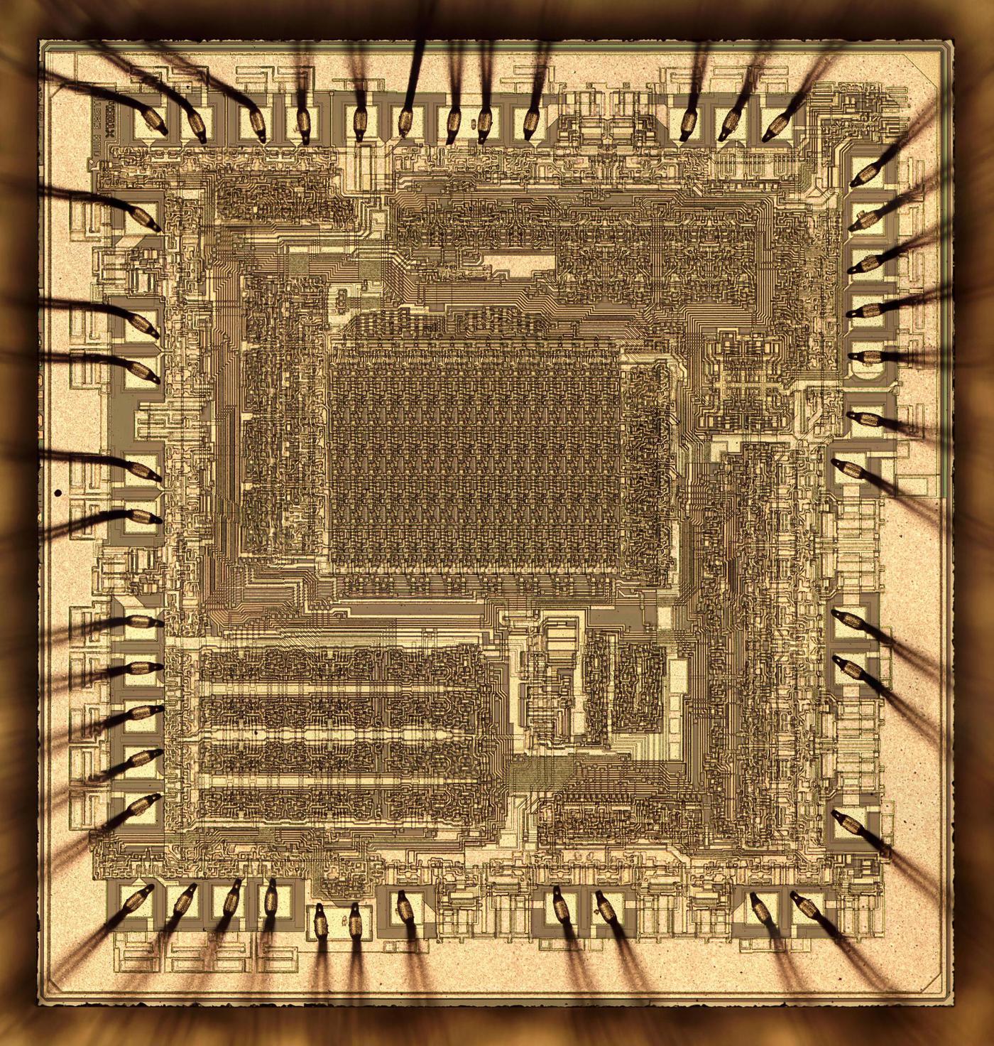
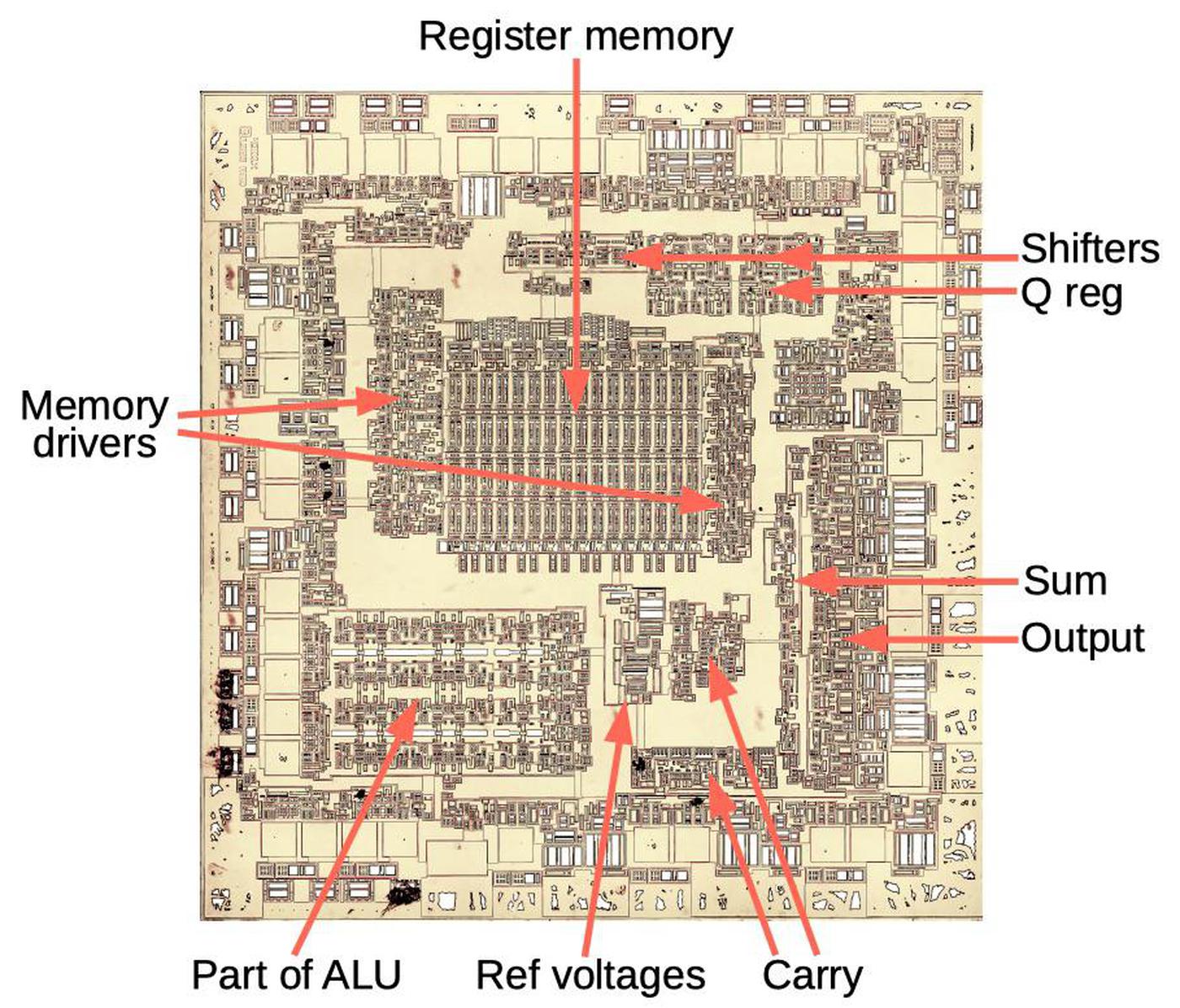
The photo below shows the Am2901 die, with key functional blocks labeled.7 For this photo, I removed the metal layers so you can see the silicon and the transistors.8 The largest functional block of the chip is the register memory in the center. The chip has sixteen 4-bit registers. (If you look closely, you can see 16 columns and 4 rows in the memory array.) To the left and right of the memory block are the memory driver circuits that read and write the memory.
The chip's arithmetic-logic unit (ALU) performs arithmetic operations (addition or subtraction) or logical operations (And, Or, Exclusive-or). The first section of the ALU is a large block in the lower left of the chip; it consists of four rows since it is a 4-bit ALU. The ALU also contains logic to generate the carry outputs for addition, using a fast technique called carry lookahead.9 Next, the ALU uses the carry values to generate the sum in parallel. Finally, the output circuitry processes and buffers the sum and sends it to the output pin.
The empty squares near the edge of the chip are the pads that connect the chip to the outside world. Next to the pads is the circuitry to send and receive signals. In particular, since the chip communicates with external circuits using TTL signals, but uses ECL circuitry inside, this circuitry converts between TTL and ECL voltages.
The chip has two shifters that can shift a word one bit to the left or right. The Q register is a 4-bit register built from flip flops. Finally, the reference voltage circuitry generates the precision voltage references required by the ECL logic.
How to see the die
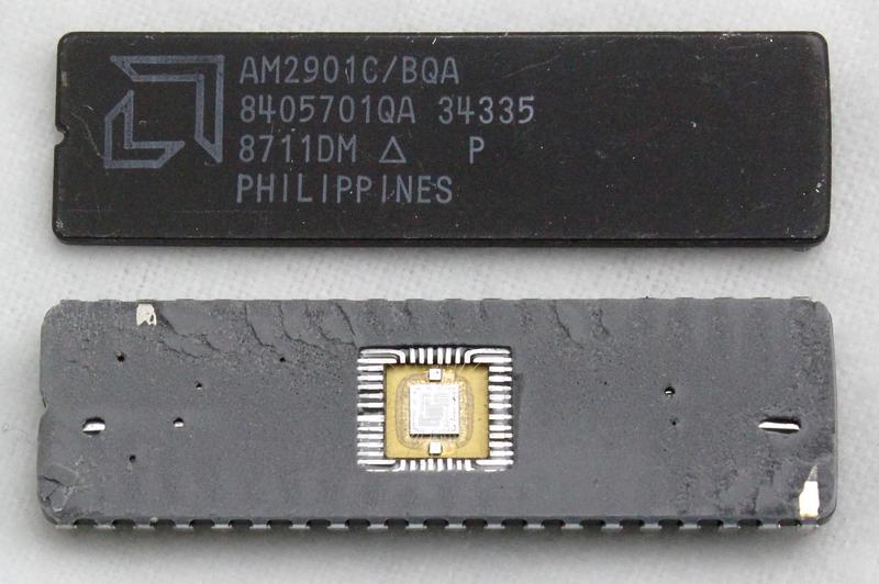
To see what's inside a chip usually requires dissolving the plastic case with dangerous acids. However, I bought an Am2901 chip that came in a ceramic package instead of plastic. By simply tapping the chip's seam with a chisel, I popped the two halves of the chip apart, exposing the die inside. The silicon die is the small square in the center of the chip. Thin bond wires connect the pads on the die to the lead frame, which goes to the 40 external pins of the chip.
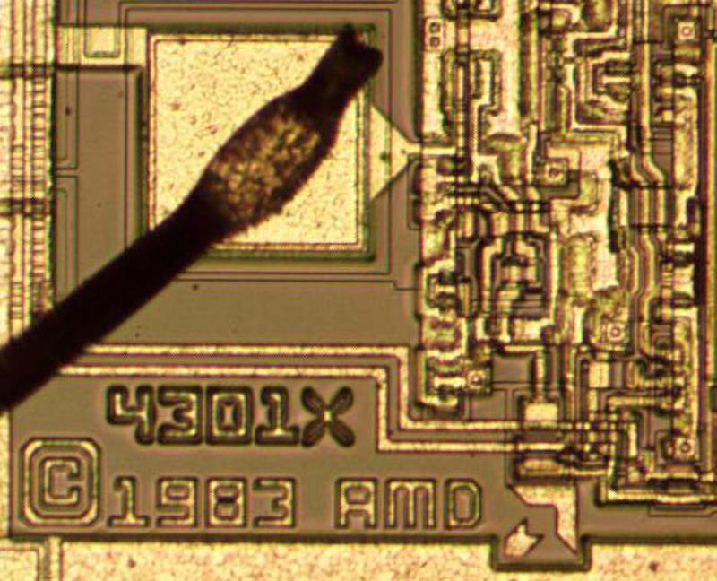
I used a special type of microscope called a metallurgical microscope to take high-resolution photographs of the chip. The photograph below shows the AMD logo. Above is a bond wire connected to a pad. The chip has two layers of metal wiring up the circuitry, visible to the right.
I stitched together multiple microscope photos to create the high-resolution images. I describe my process for creating die photos in more detail here. I then removed the metal layers8 and created another set of images of the silicon.
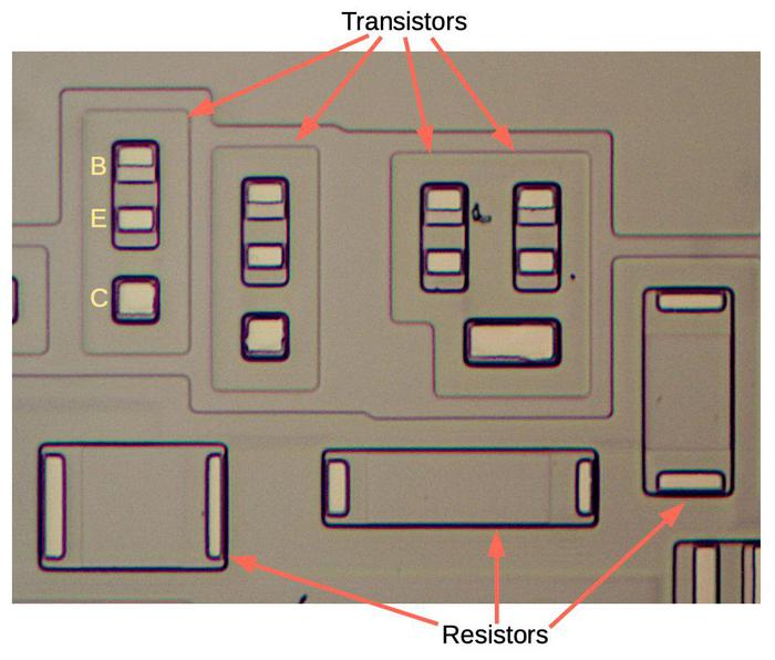
The photo below is a closeup of the silicon, showing four transistors and three resistors. Parts of the silicon are "doped" to give them different properties, and the different doping regions are visible under the microscope. This chip is built with bipolar NPN transistors, different from the MOS transistors in modern computers. The transistor on the left has the base (P-type silicon), emitter (N-type silicon), and collector (N-type silicon) labeled. The whiteish rectangles are the contacts between the silicon and the metal layer which was on top before being removed. The two transistors on the right share a single large collector. On this chip, it is common for multiple transistors to share the collector.
At the bottom are three resistors. A resistor is produced by doping the silicon to increase its resistance. Resistors on integrated circuits generally have poor accuracy. They are also relatively large; these ones are the same size as transistors, while other resistors are even larger. For these reasons, integrated circuit designs try to minimize the number of resistors.
Emitter-coupled logic
Logic circuits can be built in a wide variety of ways. Almost all computers today use a logic family called CMOS (complementary metal-oxide-semiconductor), building gates out of MOS transistors. In the minicomputer era, TTL (transistor-transistor logic) was very popular. Emitter-coupled logic (ECL) was a faster,10 but less common logic family. A disadvantage of ECL was its higher power consumption. (Circuitry in the Cray-2 supercomputer (1985) had to be immersed in Fluorinert coolant because the ECL gates gave off so much heat.)
The first versions of the Am2901 used TTL logic, but in 1979 AMD introduced a faster version, the Am2901C. The Am2901C used ECL logic internally for speed, but supported TTL voltages externally, allowing it to be easily used in TTL computers. The Am2901C, the ECL version, is the one in this blog post.
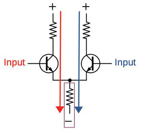
ECL is based on a differential pair, similar to the circuit inside an op-amp. The idea behind a differential pair (below) is that a fixed current flows through the circuit. If the left input is a higher voltage than the right, the left transistor will turn on and most current will flow through the left branch. Conversely, if the right input is a higher voltage than the left, the right transistor will turn on and most current will flow through the right branch. (Note that the emitters of the transistors are coupled together, thus the name emitter-coupled logic.)
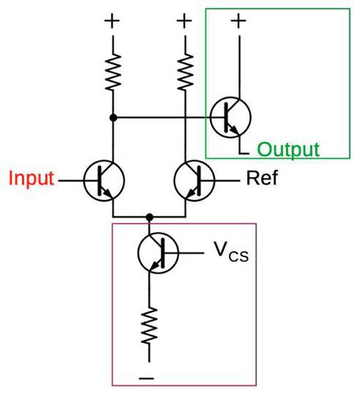
A few modifications turn the differential pair into an ECL gate. First, the voltage into one branch is fixed at a reference voltage, midway between the "0" level and the "1" level. Thus, if the input is higher than the reference voltage, it will be considered a "1", and lower will be a "0". Next, an output transistor (green) is attached to a branch to produce an output by buffering the branch's voltage. The circuit below is an inverter, since if the input is high, the current through the left resistor will pull the output low. To improve performance, the bottom resistor has been replaced with a current sink (purple), built from a transistor and a resistor.11
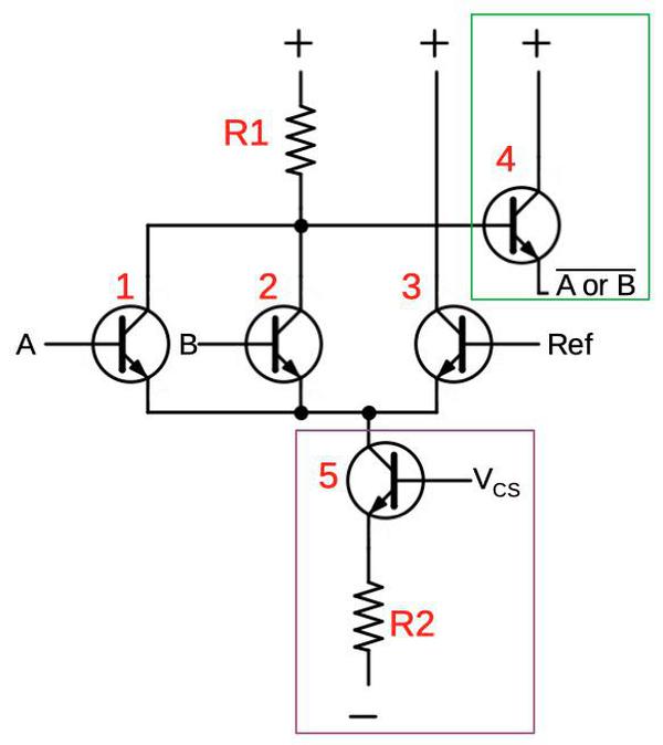
A more complex ECL gate can be created by adding more inputs. In the circuit below, a second input transistor (2) has been added in parallel with transistor 1. The current will go through the resistor R1 if input A or input B are 1 (i.e. higher than the reference voltage). In this case, the output is pulled low, creating a NOR gate. Other circuit configurations can implement AND gates, XOR gates, or more complex logic circuits.12
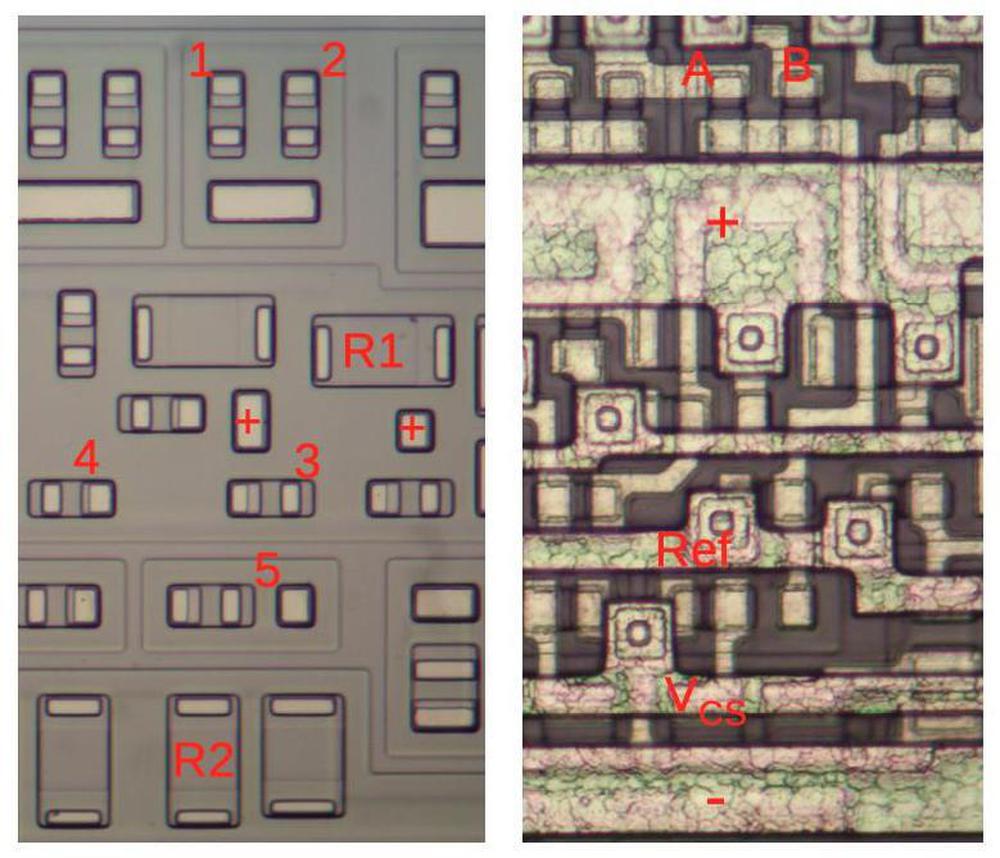
The schematic above shows a NOR gate as implemented on the chip. The photos below show the corresponding physical layout of the gate. On the left is the silicon layer of the die, showing the transistors and resistors. The photo on the right shows the metal wiring for the same part of the chip. At the top of the photo, transistors 1 and 2 receive the inputs to the gate. Each transistor has its base at the top and emitter in the middle. The transistors share a collector, the white rectangle below. The resistors R1 and R2 are the indicated rectangles of silicon. The transistors in the middle (including 3 and 4) all share a collector, connected twice to the positive voltage. (The non-numbered transistors and resistors are parts of other gates.)
Looking at the wiring on the right, the top layer provides horizontal wiring for the positive supply voltage, reference voltages, the current sink voltage VCS, and the negative (ground) supply voltage. (Note that the suppy and ground are much wider to support higher current.) Underneath this is the wiring connecting the transistors together. At the top, the inputs A and B are wired to the transistor bases. It's harder to trace out the other wiring as it is obscured by the top layer. But, for instance, you can see the connection between transistor 4, the collector of transistors 1 and 2, and R1. By studying the die photos carefully, one can determine all the wiring and reverse-engineer the chip's logic.
The Arithmetic-Logic Unit (ALU)
The arithmetic-logic unit (ALU) in the Am2901 chip performs 4-bit arithmetic or logical operations. It supports 8 different operations: addition, subtraction, and bitwise logic operations.17 (Note that it does not perform multiplication or division.)
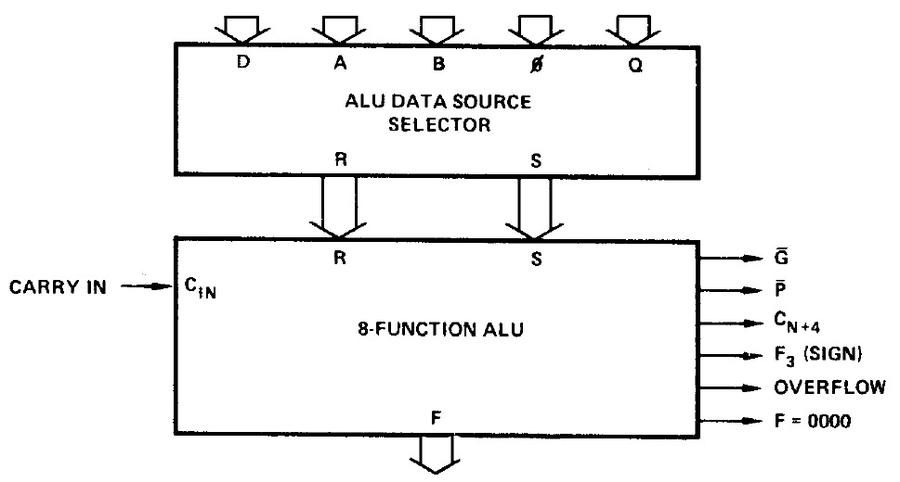
The block diagram below shows the structure of the Am2901's ALU. First, a selector (multiplexer) selects the two inputs to the ALU from the potential sources. "D" is the value fed into the chip's data pins, typically the processor's data bus. (This data first goes through circuitry to convert the external TTL voltage levels used to the ECL voltage levels inside the chip.) "A" is the value of one of the 16 entries in the chip's register file, selected by pins A0-A3, and "B" is similar. The constant value 0 can be fed into the ALU. Finally, "Q" is the contents of the Q register (an extra register, separate from the register file). The multiple data sources give the chip a lot of flexibility.
The two selected values (labeled R and S) are fed into the ALU, which performs the selected operation, yielding the result (F). The ALU also takes a carry-in value and produces a carry-out value (CN+4); these allow multiple ALUs to be combined for larger words. The G and P outputs are used for carry lookahead, while the other sign, overflow, and zero outputs can be used as condition codes in a processor.
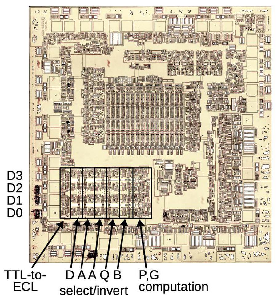
I'll give a brief explanation of the ALU circuitry, starting with the selector. The first two selector boxes below (D and A) select the ALU's first argument, while the last three (A, Q, and B) select the ALU's second argument. Each selector box implements the function Select · (Value ⊕ Invert), where Value is a potential input value, Select is 1 to select that value, and Invert is 1 to invert the value. (Since the ALU is four bits wide, four bits are selected. Each selector box is implemented with four ECL gates; see the footnote for details.13) By enabling one of the Select lines, the desired value is selected. If no Select line is enabled, the value to the ALU is 0.12 Note that the selector can also invert the input; the chip performs subtraction by adding the inverted value.
Once the two ALU inputs have been selected, the ALU computes "Propagate" (P) and "Generate" (G) bits for each pair of input bits. This is part of the carry lookahead,9 used for high-speed addition.
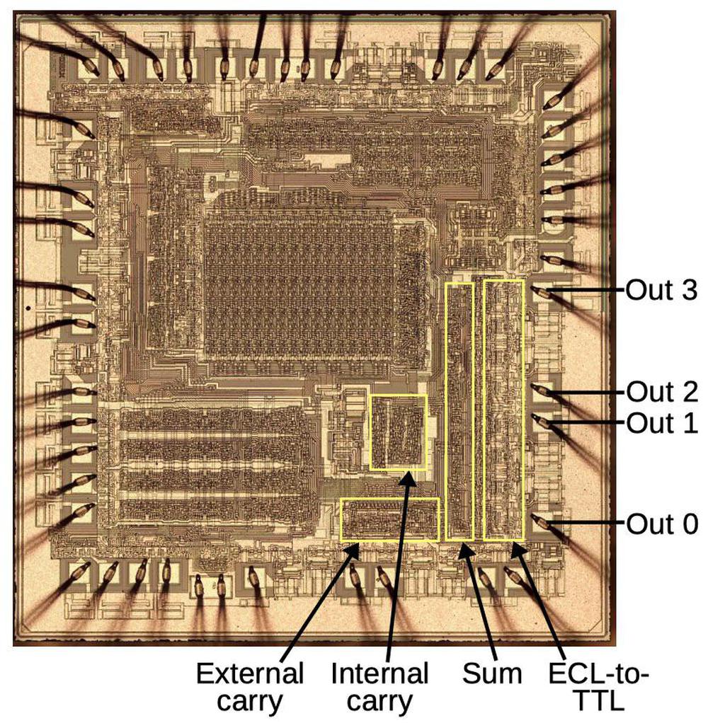
The photo below indicates the remaining parts of the ALU circuitry. (For variety, this die photo shows the metal layer, while the previous showed silicon.) The P and G signals from the previous circuit go to two blocks of carry computation circuitry. The lower carry block computes external P, G, and carry signals that provide carry lookahead across multiple chips; this allows fast addition for larger words.14 The upper carry block computes the carries that are used internally. The "sum" circuitry computes the sum for each bit using the carry, P, and G values. The important thing is that the sum for each bit can be computed in parallel, thanks to the carry lookahead. Finally, the output circuitry converts the internal ECL signals to TTL signals and drives the four output pins.15
The chip uses some interesting techniques to reuse the adder hardware for its eight operations. The selector circuit described earlier can optionally complement its input. This is used for subtraction, as well as for some logic functions. To perform logic operations (instead of addition/subtraction), the carry computation is disabled. (For a logic operation, each bit position is unaffected by what happens in other bit positions.) Finally, the adder's EXCLUSIVE OR circuit is turned into AND by forcing the P signals high.16 Thus, instead of using eight different circuits for the ALU's eight operations, the chip uses a single circuit with a few carefully-chosen tweaks. 17
Conclusion
The Am2901C chip is interesting because it is an example of high-speed ECL circuitry, a relatively uncommon logic family. The chip's ALU is spread across the lower half of the chip, implementing eight different functions and using carry lookahead for high performance. Although the chip is complex, it can be reverse-engineered with careful examination under a microscope.
Bit-slice processors such as the Am2901 were used in minicomputers and many other systems in the 1970s and 1980s. Eventually, though, improvements in CMOS technology permitted a fast processor to be implemented on a single chip, rendering the bit-slice processor obsolete. While the Am2901 had maybe a thousand transistors and ran at 16MHz, AMD now makes processors that have billions of transistors and run at 4GHz.
Follow me @kenshirriff for more reverse engineering. I also have an RSS feed.
Notes and References
-
Microprocessors on a single chip existed at the time, but they used MOS transistors that were slower than the bipolar transistors used in most minicomputers. They also generally had smaller word sizes. Eventually, CMOS processors became faster than bipolar processors; CMOS is what almost all computers now use. ↩
-
The Atari Battlezone documentation (p40) doesn't refer to the Am2901 explicitly, but gives it the Atari part number 137004-001 and calls it a "Transistor Array". Moreover, the schematic (p9) obfuscates the Am2901 pinout, showing 20 address pins and 8 data pins, so it looks like a ROM. (In contrast, all the 7400-series chips are described accurately.) Perhaps Atari was attempting to prevent cloning of the video games by hiding the identity of a few key chips. ↩
-
A popular alternative to the Am2901 in many minicomputers was the 74181 ALU chip. This provided arithmetic and logic functions, but not the registers of the Am2901. ↩
-
Some complications arise in bit-slice processors, since the slices aren't entirely independent. For instance, when adding two numbers, the carry from one slice needs to be passed into the next slice. Operations such as determining the sign of a number or testing if a number is zero, also require the slices to cooperate. The Am2901 has outputs to support these functions. ↩
-
For a detailed discussion of bit-slice processors, see Introduction to designing with the Am2901. ↩
-
Is the Am2901 a microprocessor? In my view, the Am2901 is part of a processor and not a complete microprocessor, but it depends on your definition of a microprocessor. I've written a lot more about these definitions in The surprising story of the first microprocessors. Interestingly, the Soviet Union leaned much more towards bit-slice processors (instead of single-chip microprocessors) than the US. While "microprocessor" usually referred to a single-chip processor in the West, bit-slice and single-chip microprocessors weren't really distinguished in the Soviet Union. (According to "Microcomputing in the Soviet Union and Eastern Europe".) ↩
-
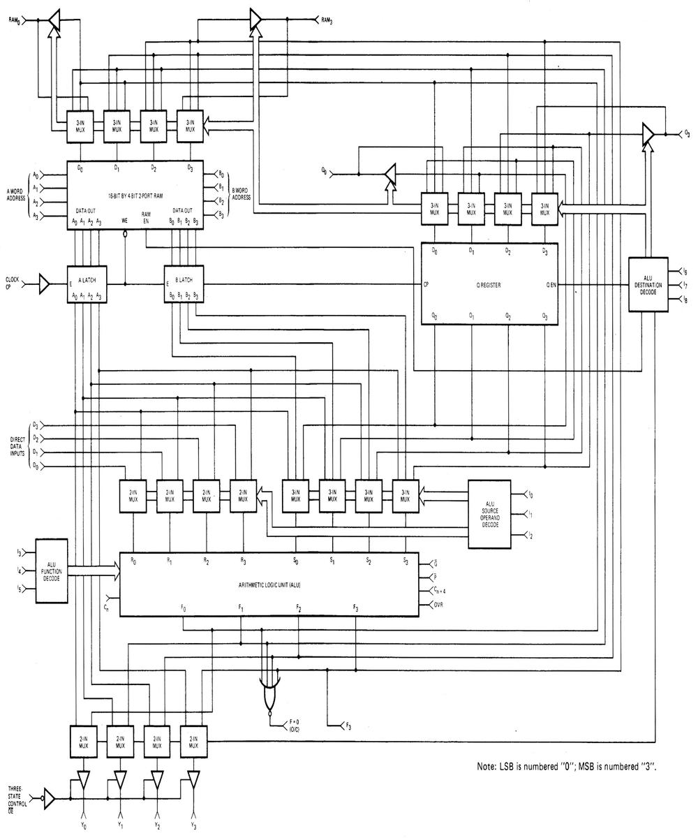
A full block diagram of the Am201 is below. (Click this or any other image for a larger version.) Note that the multiplexers above the RAM and the Q register implement a 1-bit left shift or right shift; they are labeled as "shifters" on the die photo. The multiplexers above the ALU in the block diagram are physically part of the ALU circuitry on the die.
Block diagram of the Am2901, from the datasheet. -
To remove the metal layers from the chip, I alternated applications of Armour Etch to remove the silicon dioxide layer and hydrochloric acid (pool acid) to remove metal. ↩↩
-
Carry lookahead uses "Generate" and "Propagate" signals to determine if each bit position will always generate a carry or will propagate an incoming carry. For instance, if you're adding 0+0+C (where C is the carry-in), there's no way to get a carry out from that addition, regardless of what C is. On the other hand, if you're adding 1+1+C, there will always be a carry out generated, regardless of C. Finally, for 0+1+C (or 1+0+C), there will be a carry out propagated if there is a carry in. Putting this all together, for each bit position you create a G (generate) signal if both bits are 1, and a P (propagate) signal unless both bits are 0, using simple logic gates.
The formula for computing the carry depends on the bit position. For instance, consider the carry from bit 0 to bit 1. This carry will occur if if P0 is set (i.e. a carry is generated or propagated) and there is either a carry-in or a generated carry. So C1 = P0 AND (Cin OR G0). Higher-order carries have more cases and are progressively more complicated. For example, consider the carry in to bit 2. First, P1 must be set for a carry out from bit 1. As well, a carry either was generated by bit 1 or propagated from bit 0. Finally, the first carry must have come from somewhere: either carry-in, generated from bit 0 or generated from bit 1. Putting this all together produces the function used by the Am2901: C2 = P1 AND (G1 OR P0) AND (C0 OR G0 OR G1). Formulas for the various carries and external P, G, and carry are given in the datasheet, Figure 9. ↩↩
-
ECL gates obtained much of their speed advantage because the transistors were not completely turned on (i.e. saturated). This allowed the transistors to switch the current path rapidly. Additionally, the difference between a "0" voltage and a "1" voltage was small (about 0.8) volts, so signals could switch between the two voltages quickly. In comparison, TTL gates typically had a difference of about 3.2 volts between a "0" and a "1", requiring more time to switch. (Signals could typically switch at about 1 volt per nanosecond, so a larger voltage swing caused nanoseconds of delay.) On the other hand, the small voltage swings of ECL made the circuits more sensitive to electrical noise. ↩
-
The current sink at the bottom of the ECL gate provides an essentially-constant current, controlled by the input voltage VCS. This is an improvement over a simple resistor, since the current through the resistor varies based on the voltage across it, which depends on the input voltages. The current sink circuit also saves space by using a smaller resistor. ↩
-
The outputs of the ALU select gates are connected together with a wired-OR. The unselected values output 0, so the value on the wire is the desired one. In this way, the circuit implements a multiplexer with minimal circuit. ↩↩
-
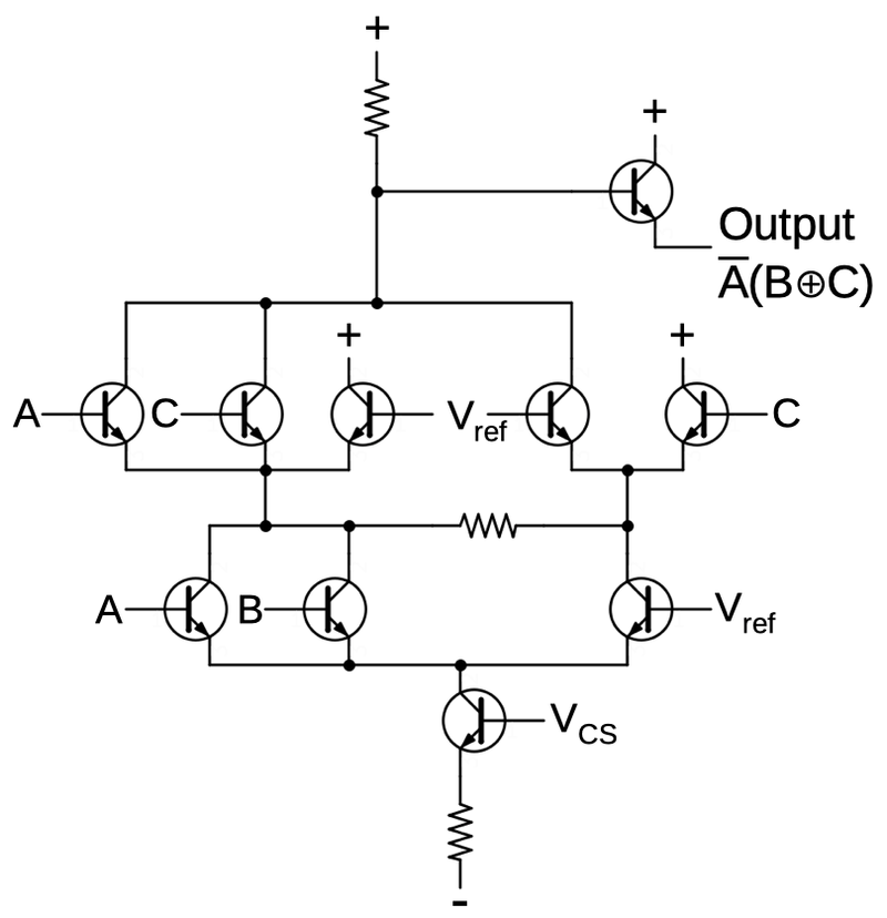
The diagram below shows the AND-XOR circuit used in the AM2901 ALU that implements A' · (B ⊕ C). I'll briefly explain its operation. If input A is high, current flows through the leftmost transistors, pulling the output low. If B and C are both high, current through the left B and C transistors pulls the output low. If B and C are both low, current through the Vref transistors pulls the output low. If B and C are different, the current is sourced from on the "+" transistors so the output remains high. The key point is that a single ECL gate can implement a complex function; in contrast, XOR is difficult with most logic families. (I find ECL logic reminiscent of 1920s-era relay logic because it switches between two paths, rather than switching on or off.)
Schematic of an ECL AND-XOR circuit. It is slightly simplified: the input voltage levels for the lower half need to be a diode drop lower than the upper inputs. I'm not sure of the purpose of the horizontal resistor.The only reference I've found for complex ECL circuits is The VLSI Handbook chapter 38. ↩
-
The carry lookahead techniques can be implemented across multiple chips for fast additions larger than 4 bits. Each chip generates a Generate and Propagate signal, indicating if that chip will generate a carry or propagate a carry-in. These signals are combined by a look-ahead carry generator chip such as the Am2902 look-ahead carry generator chip. ↩
-
The output circuitry also includes multiplexers; the chip can either output the ALU result or the A register value. ↩
-
The chip uses the P and G values to generate the sum of inputs R and S with carry-in C. The sum is (R ⊕ S ⊕ C)', computed as ((P' ∨ G) ⊕ C)', where P = R∨S and G = R•S. If P is forced to 1, (P' ∨ G) reduces to G, which is R•S. Thus, by changing P, the same circuit can be used to compute the AND of the inputs R and S. ↩
-
The table below shows the eight operations that the ALU can compute. Three of the instruction bits fed into the chip are used to select the operation: I5, I4, and I3. The "Function" column in the table shows the function as documented, while the "Computation" column shows how each bit of the function is computed internally. First, note that the operations all boil down to EXCLUSIVE OR (⊕) or AND (∧). Addition is performed by bitwise EXCLUSIVE OR of the two arguments and the carry bits. Subtraction is performed by complementing an argument and then adding. For example, adding the complement of R (R') is the same as subtracting R. Bit I3 complements R, while bit I4 complements S. Note that the EXCLUSIVE OR operations (EXOR and EXNOR) use the same circuitry as addition, but carry computation is blocked. The AND operation is performed by blocking the G signal. Finally, OR is computed using De Morgan's law, which shows that R' ∧ S' = (R ∨ S)'. The point of this is that the Am2901 doesn't need separate circuitry for addition, subtraction, AND, OR, and EXCLUSIVE OR, but reuses most of the circuitry.
↩↩Mnemonic I5 I4 I3 Function Computation ADD 0 0 0 R Plus S R ⊕ S ⊕ Carry SUBR 0 0 1 S Minus R R' ⊕ S ⊕ Carry SUBS 0 1 0 R Minus S R ⊕ S' ⊕ Carry OR 0 1 1 R OR S (R' ∧ S') ⊕ 1 AND 1 0 0 R AND S R ∧ S NOTRS 1 0 1 R' AND S R' ∧ S EXOR 1 1 0 R EX OR S R ⊕ S' ⊕ 1 EXNOR 1 1 1 R EX NOR S R' ⊕ S' ⊕ 1
26 comments:
I remember Apollo wanted to ship MC68020-based workstations before the chip was actually available. Their solution was to grab a stack of AM2900s and emulate the MC68020, so their existing software still ran without modifications.
It was quite a stack of hardware - two or three lunch tray sized boards to replicate one chip.
Even computers built from many chips or discreet transistors can be designed in a bit slice way so you can have several boards be exactly alike instead of having every one be unique.
The CHM has a photo of the Apollo AM2900 based CPU (emulating the MC68020 processor). There are nice neat rows of eight AM290x chips, 8 x 4 = 32 bits.
https://www.computerhistory.org/collections/catalog/102681229
J. Peterson: The Apollo workstation you mention actually emulated the 68000, not the 68020. Source: I was in the Motorola 68000 design group from 1985 to 1996. The first project I worked on was the 68030, which was essentially the 68020 with an integrated MMU and virtual memory capability. We did have a full hardware breadboard of the 68020. The 68030 breadboard was 18 24"x24" wirewrap breadboards, each with a 23x14 array of 20 pin DIP sockets! The chips were mostly PALs and RAM/ROM, no bitslice. This was before software logic simulation was a real thing.
@CaptainTivo
Wow, I had no idea that they actually mocked up processors in hardware while designing them. Especially in the 80s when they were at that level of complexity. I'd love to see a picture of one of those wirewrap breadboards if it exists. I presume they did not run at the speed the final product was intended to run at.
hi Ken, great article ... as always. A very minor correction, the Cray 2 and Cray 3 were cooled via liquid Fluorinert. It was the Cray 1 and Cray X-MP that were cooled via freon. Hopefully, you'll find an opportunity to write an in-depth article on some aspect of the early Cray designs, either logic, power supply or cooling ... all amazing for their time ... regards andyg
I used the AMD 2901 in 1978 to design a 32-bit computer for Systems Engineering Labs in Florida. Most minicomputers at the time were 16-bit wide made by DEC, Data General and Prime who were all located in the Boston area. The 2901 was a big improvement over the TI 74181 but the chip itself is wider (.6 inch) versus the usual .3 inch wide packaging of the 74XX series TTL chips. This made prototyping initially difficult. The board I designed was 30 x 30 inches crammed full of several hundred chips. Separate boards were for the computer's memory and they used the ubiquitous 1103 dynamic memory chip.
Josh O. As it happens I do have some pix of the 68030 breadboard. Normally I would not have been allowed to take pictures of this, or even bring a camera into the building, but I gave a talk on the 68030 at Stanford in 1986 and I got permission to take these pix.
I did not work on the emulator (that was the Tiejen brothers), I did design on the TLBs.
As far as I remember the emulator ran less than 1 MHz. But remember, the 68030 design target was 16 MHz (yes, megahertz).
Here are the pix: https://drive.google.com/open?id=1ZtULPYBnZ2ZnI8LJavVCWvJ2v2n0UO8J
The cards were about 24" on a side, with 20 pin wirewrap DIP sockets. Mostly PALs, RAMs and ROMs. Although the 68020 and 68030 have relatively complex instruction set, a lot it was implemented in microcode, so the actual logic is quite as hairy as you might think.
The 3 Mbps Experimental Ethernet interface card in the original Stanford University Network (SUN) project machine used three of the Am2901s to implement a 12-bit bit-slice machine to handle the decode and encode of the Ethernet signaling. Not sure exactly who developed the card, but I assume that it was Andy Bechtolsheim since he was the primary developer for the original SUN hardware cards.
CaptainTivo: your 68030 pics are very interesting. I think people would like to see them so may I share them? Also, do you have a copy of your talk?
In the early 80's I worked for a startup that used this to extend the Z-80 Instruction set to add a wider word to support 2-d graphics at much higher speed than was possible before. Was a lot of fun, worked well, died when the IBM PC changed price points for computers and company was too stuck on making systems to pivoting to making graphic cards.
Ken Shririff, sure you can post if think they are of interest. I actually have a few more of the station showing the test equipment and the ExorMACSS chassis (the 68000 development computer) which I will put in the shared folder. I don't have my foils (remember those) from the talk. I'm surprised I kept the 8x10 color glossies :-)
I used the 2900 series in quite a few systems. One of them was a DG Nova knock-off that out performed the Nova computer. I loved the 2900 series and was disappointed to see it gone from the market!
These chips were used in the HP-9845C color monitor (to do vector plot, etc) and in the option 200 processor upgrade for the same 9845C and 9845B. The bit slice processor upgrade gives a 6X boost in processing speed. I have both, but the monitor is currently not working.
I worked on a 2901/2910 system as part of a EE class at UIUC back in the dark ages. As I recall they were multibus wire wrap cards, retired shortly after I graduated.
Strange timing. I started working on getting parts of the AM2900. I've only have a AM2901 running so far. I've enjoyed the write up of its internals.
I wrote microcode for a 32-bit system (never shipped) from Basic Four Corporation (aka MAI Corporation) that was built with 2901s.
One thing you didn't mention: AMD had absolutely totally excellent best-ever-I've-seen design notes - including a full 7- or 8- part tutorial! - on building systems with the 2901. The tutorial, IIRC, went from basic knowledge all the way through to schematics of a complete working CPU. (I still kick myself for getting rid of my set of AMD documentation sometime in the 90s ...)
This one might be very interesting for you:
http://www.donnamaie.com/AMD_Vintage/AMD_2900_ED2900A.html
Still a fascinating chip... AMD had a great technical note explaining how to build a much faster Am9080 (Intel 8080) out of these. I used that to implement it in VHDL: https://github.com/zpekic/sys9080
I used Am2900 - Family chips to build a LISP machine. Good old days...
I just found out that the 2901 was used in the Eventide Reverb box from 1982, the SP2016.
It had six 2901 inside! https://cdn.eventideaudio.com/uploads/2021/07/SP2016-Manual-Original.pdf
We designed a couple of graphics computers using 2900 series in 1982 - Z80 instruction set combined with inline instructions for computre graphics for Florida Computer Graphics startup. Died after PC came out and we couldn't comvince management to pivot to graphics cards. Missed opportunity.
It is really 4 TI 74181 in one chip. Did a design at work in late 1970's using part. Later replace part with a TI DSP 320/325 processor.
I remember first encountering this chip when I was writing and emulator for the Atari I-Robot arcade game. I-Robot was the first arcade game to use 3D filled polygons so it had a custom processor built around 4 2901s for doing all the 3D transformation and projection calculations. It was a pretty elegant design using just microcode for the program and a minimum of other components.
Another great article Ken. I like the comments describing various projects using the 2901. Atari loved to use it. Star Wars Arcade used a few for the so called Math Box.
Dan Boris, do you remember off hand what the clock speed of the I, Robot Mondo Condo bit slice processor was? I read somewhere that it was scalable per instruction, so big instructions would up the speed. Quite amazing if true.
Furthermore the controller was custom and not an AMD part. Do you have any comments regarding that?
Post a Comment