 and a counterfeit charger (right")
From the outside, the real charger (left) and counterfeit charger (right) are almost identical. If you look very closely, you can spot are a few differences in the text: The counterfeit removed "Designed by Apple in California. Assembled in China" and the manufacturer "Foxlink"[1], probably for legal reasons. (But strangely, the counterfeit still says "TM and © 2010 Apple Inc.") The counterfeit charger displays a bunch of certifications (such as UL) that it doesn't actually have. As you will see below, there is no way it could pass safety testing.
Opening up the chargers reveals big differences between them. The genuine charger on the left is crammed full of components, fitting as much as possible into the case. The counterfeit charger on the right is much simpler with fewer components and much more empty space. The Apple charger uses larger, higher-quality components (in particular the capacitors and the transformer); below you will see that these have a big effect on power quality and safety.
 and a counterfeit charger (right).")
One safety difference is obvious: the Apple charger has much more insulation. The upper (high-voltage) half is wrapped in yellow insulating tape. Some components are encased in shrink tubing, there are plastic insulators between some components, and some wires have extra insulation. The counterfeit charger only has minimal insulation.
The build quality of the Apple charger is much higher. In the counterfeit charger, some components are visibly crooked or askew. While this doesn't affect the circuit electrically, it indicates a lack of care in construction.
Flipping the boards over reveals that the circuitry of the genuine Apple charger is much more complex than the counterfeit. The Apple board is crammed with tiny surface-mounted components in every available spot. The counterfeit board has a lot of empty space, with just a few components. Note the reddish insulating tape in the lower center of the Apple board, another safety feature of the genuine charger.
 and a counterfeit charger (right).")
How the chargers work
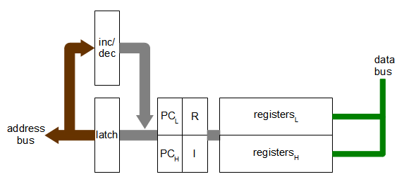
Both the real and counterfeit chargers use similar flyback[2] switching power supply circuits. The switching power supply is the innovation that allows these chargers to be so compact, unlike the heavy "wall warts" powering older consumer electronics. The principle of a switching power supply is the power is switched on and off tens of thousands of times a second, allowing it to provide the exact amount of power required with very little power wasted as heat. In addition, the high frequencies allow the charger to use a small transformer, unlike the bulky transformers used for 60 Hz AC.Since the counterfeit charger is much simpler, it is easier to understand how it works and I'll explain it first in reference to the picture below. The AC power enters through the white wires in the upper left. It passes through a fusible resistor, which acts as a safety fuse. Below this, the bridge rectifier contains four diodes which convert the AC into DC (at about 170 to 340 volts[3]). The input capacitor smooths out this power. The 4-pin control IC[4] monitors the charger and uses the switching transistor to turn the high-voltage DC on and off 41,000 times per second. This chopped DC is fed into the primary winding of the flyback transformer. The transformer converts this to the desired high-current 5 volts. The output diode produces DC, and the output capacitor smooths it out. Finally, the output voltage is available at the USB connector to power your iPad. A few components round out the circuit. A feedback winding on the transformer provides voltage feedback to the control IC. This winding also powers the IC; the IC power capacitor smooths out this power. Finally, the blue snubber[5] capacitor absorbs current spikes when the transistor is switched off.[6]

The genuine iPad charger below operates on similar principles, although the circuit is more advanced. The AC input is on the lower right, and goes through a 2A fuse (in black insulation for safety). The primary has much more filtering than in the counterfeit charger with a filter coil (common mode choke), inductor, and two large electrolytic capacitors. This increases the cost, but improves the power quality. On the output side (left), the charger has two filter capacitors, including a high-quality aluminum polymer capacitor (with the magenta stripe). The Y capacitors help reduce interference.[7] The tiny NTC temperature sensor lets the charger shut down if it overheats. (I removed some of the charger's insulation to make the components visible in this photo.)

On the other side of the circuit board, things get complicated in the Apple charger. Starting with the AC input in the upper right, the charger includes additional input filters as well as spark gaps.[8] The latch release circuit[9] lets the charger reset quickly from faults. The control IC[10] provides advanced control of the charger under varying conditions. (This IC is much more complex than the control IC in the counterfeit charger.) The current sense resistor lets the IC monitor the current through the transformer and the line voltage resistors let the IC monitor the input voltage (as well as initially powering-up the IC[9]). The protection circuit uses the temperature sensor on the other side of the board to shut down if there is an over-voltage or over-temperature problem. [20]

The secondary side includes some special features for power quality. The Y-capacitor filter works with the Y capacitors to filter out noise. The output filter circuitry is more complex than in the counterfeit. Note that the real charger has a ground connection, unlike the counterfeit charger which has a plastic pin here.[11]
Both chargers use resistors to put special voltages on the USB data lines[12] to indicate the charger type, using Apple's proprietary system (details). (This is why iPads say "Charging is not supported with this accessory" with some chargers.) Through these resistors the genuine charger indicates that it is an Apple 2A charger, while the counterfeit indicates that it is an Apple 1A charger. This shows that the counterfeit is really a 5W charger packaged as a 10W charger.
When looking at these circuits up close, it's easy to forget just how small the components are. The picture below shows one of the surface-mount components (a 0-ohm resistor[13]) from the iPad charger. It is just to the left of Roosevelt's chin on the dime.

Safety, or lack thereof
Safety probably isn't something you think about when you plug in your charger, but it's important. Inside the charger is 170 volts or more with very little separating it from your iPad and you. If something goes wrong, the charger can burn up (below), injure you, or even kill you. Devices such as chargers have strict safety standards[14] - if you get a charger from a reputable manufacturer. If you buy a cheap counterfeit charger, these safety standards are ignored. You can't see the safety risks from the outside, but by taking the chargers apart, I can show you the dangers of the counterfeit.

Creepage and clearance
The UL regulations[14] require safe separation between the high voltage and the low voltage. This is measured by creepage - the distance between them along the circuit board, and clearance - the distance between them through air. The regulations are complex, but in general there should be at least 4mm between high-voltage circuitry and low-voltage circuitry.
 and low-voltage side (top).")
The image above shows how the genuine iPad charger's circuit board separates the high voltage (bottom) from the low voltage (top). The happy face on the right marks an empty region that provides a safety gap between the primary and secondary. (This is a contrast with the rest of the circuit board, which is crammed full of components.) This gap of 5.6mm provides a comfortable safety margin. The happy face on the left marks a slot in the board that separates the low voltage and high voltage. The photo below shows how an insulating fin is built into the case and through this slot to protect the USB connector. Additional reddish-brown insulating tape goes through this slot, and the whole high-voltage section is wrapped in yellow insulating tape. The result is multiple layers of protection.

The creepage distance on the counterfeit charger board below is scary - only 0.6 mm separation between low and high voltage. The sad face on the right shows where a low-voltage trace is nearly touching the high-voltage trace below. (The ruler on the right indicates millimeters.) The board isn't as bad as it could be: the happy face on the left marks a slot cut in the circuit board under the transformer to increase the creepage distance. But overall, this board is unsafe. If you use the charger in a humid bathroom and a drop of water condenses across the 0.6 mm gap, then zap!

Safety in the transformer
For safety, the high-voltage and low-voltage sides of the charger must be electrically isolated.[15] But obviously the electrical power needs to get through somehow. The flyback transformer accomplishes this task by using magnetic fields to transfer the power without a dangerous direct connection. Because the transformer is a large and relatively expensive component, it is tempting to take safety and quality short cuts here. The genuine transformer (left) is considerably larger than the counterfeit (right), which is a hint of better quality and more power capacity. Disassembling the transformers shows that this is the case.
 and a counterfeit charger (right). Dime and banana are for scale.")
The key safety requirement of the transformer is to separate the high-voltage windings from the low-voltage secondary winding, and the counterfeit charger fails here. The pictures below show the transformers after removing primary windings and insulating tape, revealing the secondary winding. The wires look similar at first glance, but the the genuine charger (left) has triple-insulated wire while the counterfeit (right) is uninsulated except for a thin varnish. The triple-insulated wire is an important safety feature that keeps the high voltage out even if there is a flaw in the insulating tape and in the wire's insulation. Also note the additional black and white insulation on the wires where they leave the transformer. In the counterfeit charger, the only thing separating the secondary winding from high voltage is the insulating tape. If there is a flaw in the tape or the wires shift too far, then zap!


The real charger provides much more power with much less noise
Lab measurements of the output from the chargers shows a couple problems with the counterfeit. First, the counterfeit turns out to provide at most 5.9W, not 10W. Second, the output voltage is extremely noisy and full of spikes.The following voltage-vs-current graphs show the performance of the iPad charger (left) and counterfeit charger (right) under increasing load. The line for the real charger goes much farther to the right, showing that the real charger provides much more current. By my measurements, the real charger provides a maximum of 10.1 watts, while the counterfeit charger provides only 5.9 watts. The consequence is the real charger will charge your iPad almost twice as fast. (For details on these graphs, see my article testing a dozen chargers.) The other thing to note is the line for the Apple charger is smooth and thin, while the counterfeit charger's line is all over the place. This indicates that the power provided by the counterfeit charger is noisy and low quality.


The next pair of graphs shows the power quality. The yellow line shows the voltage. The real charger has a stable yellow thin line, while the counterfeit charger's output has large voltage spikes. (I had to change the scale to get the output to fit on the screen, so the counterfeit charger is actually twice as bad as it appears here.) The bottom of the counterfeit charger's yellow line is wavy, due to 120 Hz ripple appearing in the output voltage.


The orange line shows the frequency spectrum of the output: lower is better, and higher is exponentially worse. The counterfeit spectrum is much higher in general, with a large spike at the switching frequency. This shows that the counterfeit charger's power is worse across the frequency spectrum.
You might wonder if the power quality actually matters. The biggest impact it has is on touchscreen performance. The interference from bad power supplies is known to cause the touchscreen to behave erratically.[16] If your screen malfunctions when plugged into a charger, this is probably the cause.
Inside the real charger's transformer
There's more inside the transformer that you'd expect. This section does a full teardown of the transformer from the genuine charger.


The first photo above shows that underneath the the first layer of yellow insulating tape, a layer of copper foil is attached to the transformer's ferrite core to ground it. Next, removing the ferrite core and more insulation reveals the double-stranded primary winding. The high-voltage input is fed into this winding.


Underneath the primary winding and more insulating tape is the triple-stranded bias winding, which provides feedback and power to the control IC. (In the photo, this winding has been removed and is surrounding the transformer.) After removing more insulating tape, the secondary winding of the transformer is visible. As discussed in the safety section, the secondary winding has triple-insulated wires and extra insulation where the wires leave the transformer. The next layer of insulation (right) contains copper foil. This helps reduce interference.

Finally, the innermost layer of the iPad charger flyback transformer is the second half of the primary winding (above). Splitting the primary winding into two layers is more expensive, but results in a better transformer due to better coupling of the magnetic fields.
In comparison, the transformer of the counterfeit charger is much lower quality. (I haven't included the pictures for reasons of space; click through to see them.) It simply has the bias winding (pic), secondary winding (pic), and primary winding (pic) , separated by insulating tape. Unlike the genuine transformer, the counterfeit saves cost by omitting the copper foil layers. The counterfeit also doesn't use the more expensive split, multi-stranded windings that the genuine charger uses. As discussed earlier, the secondary winding is plain copper wire, not triple-insulated wire, which is a significant safety flaw.
How does the iPad charger compare to the iPhone charger?
The iPad charger is considerably larger than the iPhone charger and provides twice the power. In my detailed iPhone charger teardown I looked at the internals of the iPhone charger. The iPhone charger (below) uses two circuit boards that combine to form a one inch cube, which is impressive engineering. The iPhone and iPad chargers are both flyback switching power supplies, but the feedback mechanisms are very different.[17] Overall, I like the iPhone charger more than the iPad charger from a design standpoint, mainly because of the harder engineering challenge of cramming everything into a much smaller space.
, Y capacitor (blue), flyback transformer (yellow), USB connector (silver). The primary circuit board is on top and the secondary board on the bottom.")
Schematics
In my iPhone charger teardown, I drew up a schematic of the charger, but for the iPad chargers I didn't need to do this. The genuine iPad charger is almost identical[18] to the reference design schematic provided by iWatt. The counterfeit charger is almost identical to the schematic in the DB02A controller datasheet. You can see from the schematics that the genuine charger has a much more complex circuit than the counterfeit. (Click the thumbnails below to get to the datasheets.)


Is the Apple charger worth the price?
Apple's charger is expensive compared to other chargers, but is a high quality product. You should definitely stay away from the cheap counterfeit chargers, as they are low quality and dangerous. Non-Apple name brand chargers are generally good quality according to my tests, with some better than Apple. If you want to get an Apple charger without the high price, the best way I've found is to buy a used one on eBay from a US source. I've bought several for testing, and they have always been genuine.I wrote earlier about Apple's huge profit margins on chargers. Apple has since dropped their charger prices from $29 to $19, which is more reasonable, but looking at the price of similar chargers from other manufacturers and the cost of components, I think Apple has a huge profit margin even at $19.[19]
In any case, the iPad charger is an impressive piece of engineering with a lot of interesting circuitry inside. The counterfeit charger is also impressive in its own way - it's amazing that a charger can be manufactured and sold for such a low price (if you don't care about safety and quality). Overall, you mostly get what you pay for; even if you can't tell from the outside, there are big differences inside the case.
Notes and references
[1] Foxlink (Taiwan), Foxconn (Taiwan), and Flextronics (Singapore) are all manufacturers for Apple with confusingly similar names. Foxconn is the company with controversy over employee treatment; this charger is made by Foxlink, a different company. Interestingly, the chairmen of both companies are brothers and the companies do a lot of business with each other. The companies state that they are entirely independent, though (statement, Foxlink annual report). Foxconn and Flextronics are the world's #1 and #3 largest electronics manufacturing companies according to the MMI top 50 for 2013, while Foxlink is smaller.[2] The chargers uses a flyback design, where the transformer operates "backwards" from how you might expect. When a voltage pulse is sent into the transformer, the output diode blocks the output so there is no output - instead a magnetic field builds up in the transformer. The transformer core has a tiny air gap to help store this field. When the voltage input stops, the magnetic field collapses, transferring power to the output winding. Flyback power supplies are very common for low-wattage power supplies.
[3] You might wonder why the DC voltage inside the power supply is so much higher than the line voltage. The DC voltage is approximately sqrt(2) times the AC voltage, since the diode charges the capacitor to the peak of the AC signal. Thus, the input of 100 to 240 volts AC is converted to a DC voltage of 145 to 345 volts internally. This isn't enough to be officially high voltage but I'll call it high voltage for convenience. According to standards, anything under 50 volts AC or 120 V dc is considered extra-low voltage and is considered safe under normal conditions. But I'll refer to the 5V output as low voltage for convenience.
[4] The counterfeit charger uses a DB02A controller IC. This controller only has four pins and is in a TO-94 (SIP-4) package. (According to the official JEDEC standard, TO-94 is a bolt-like package for large SCRs. It's a puzzle why some companies use TO-94 to describe 4-pin inline packages.) According to the datasheet (Chinese), the chip is for 500mA-1000mA chargers, which explains why the counterfeit charger only produces 5 watts, instead of the 10 watts an iPad charger is supposed to produce. This controller is very inexpensive, available for ¥ 0.35 (about 6 cents).
I couldn't find any US chips similar to this chip, even after a lot of searching; it appears to be a Chinese design with datasheets only in Chinese, manufactured by "Fine Made" Shenzhen Fuman Electronics. Since the chip only has four pins, I expected it to be a trivial Ringing Choke Converter (RCC) circuit with just a couple transistors inside the chip - but I cracked it open with Vise-Grips and it turns out to be a fairly complex chip. I took a picture through a microscope of the IC die, which is about 1 mm across. One interesting feature is the many white pads around the outside of the die, which are used to blow fuses to trim various resistances in the chip. I wasn't expecting to see this level of quality and sophistication. The die has the label "N7113 802" at the right; I don't know what this indicates. Three of the four wires connect in the lower left, and the fourth in the lower right.

[5] When a diode or transistor switches, it creates a voltage spike, which can be controlled by a special snubber or clamp circuit. For a lot of information on snubbers and clamps, see Passive Lossless Snubbers for High Frequency PWM Conversion and Switchmode Power Supply Reference Manual.
[6] In the counterfeit charger, the switching transistor is a ALJ 13003 NPN power transistor (datasheet), apparently made by Shenzhen LongJing Microelectronics Co. This transistor is a version of Motorola's MJE 13003 switchmode transistor which was introduced in 1976 (MJE indicates power device in a plastic package). The bridge rectifier is a B6M (datasheet). The output diode is a SR260 Schottky barrier rectifier.
[7] The iPad charger uses special Y-capacitors to bridge the high-voltage and low-voltage sides of the charger. This capacitor helps reduce EMI interference, and is specially designed to avoid any safety hazard. It does, however, pass a tiny amount of electricity - if you feel a tingle from your charger, these capacitors are probably the cause. For more information on X and Y capacitors, see Kemet's presentation and Designing low leakage current power supplies.
[8] The iPad has two spark gaps next to inductor L1 (the input AC common mode choke). I couldn't find a lot of information on this sort of spark gap, but one example of it is an Infineon SMPS design, where similar spark gaps are designed to discharge accumulated charge for a 3KV lightning surge test.
[9] The Apple charger includes a "latch release circuit". If there is a fault, the control IC will shut down the charger until power is removed. However, after unplugging a charger, the input capacitors may store power for many seconds. (You may have seen LEDs remain illuminated for several seconds after unplugging devices.) The latch release circuit ensures that the charger will reset properly even if you plug it back in quickly. It does this by providing a separate diode bridge for the charger's power - this circuit has a much smaller capacitor, so it will power off quickly. (See the schematic for details.) This seems like over-engineering to me, adding extra circuitry for this rare case.
In normal use, by the way, the control IC is powered by the transformer's feedback winding. But if the control IC isn't running, the transformer won't work, leading to a chicken-and-egg situation. The solution is a startup power path where the control IC gets enough power from the AC input to start up, and then switches to the transformer.
[10] The genuine charger uses a complex control chip manufactured by iWatt, the 1691. This chip monitors the input line voltage, the current through the transformer, and the voltage feedback from the transformer. It controls the switching frequency and length of time the power is switched on, with different behavior under no load, low load, and high load, as well as constant monitoring for faults. A detailed presentation on the iW1691 is here. This chip sells for about 30 cents, but I expect Apple gets a better price.
[11] The real charger has a metal ground pin that connects to the power plug, while the counterfeit has a plastic pin. This is one difference between the chargers that is visible externally if you slide the power plug off the charger. Ironically, the US plug doesn't use the ground connection, so this is one safety issue that doesn't make any difference in practice.
[12] Apple uses a proprietary technique for the charger to indicate to the device what kind of charger it is. Different types of Apple chargers use resistances to put different voltages on the USB D+ and D- pins. For details on USB charging protocols, see my earlier references.
[13] While it would be nice to find superconductors inside the charger, unfortunately the zero-ohm resistor is a bit more than 0 ohms. While this resistor may seem pointless, it allows the manufacturers to substitute a resistor later if different transistors require it.
[14] The outside of the charger has the slightly mysterious text: "For use with information technology equipment". This indicates that the charger is covered by the safety standard UL 60950-1, which specifies the various isolation distances required. For a brief overview of isolation distances, see i-Spec Circuit Separation and some of my earlier references.
[15] Only a few special components can safely bridge the gap between the high voltage side of the charger and the low voltage side. The most obvious is the transformer. Y-capacitors can also bridge the primary and secondary side because they are designed not to pass dangerous currents, and not to short out if they fail. Optoisolators use a light signal to provide feedback between the circuits in an iPhone charger, but are not used in the iPad charger.
[16] For an explanation of why the noisy output from cheap chargers messes up touchscreens, see Noise Wars: Projected Capacitance Strikes Back. The article discusses how capacitive touchscreen ICs need to sense pico-Coulombs of charge, which is very difficult when AC noise is present. The article blames touchscreen problems on aftermarket low cost chargers.
[17] The biggest difference between the iPhone charger and the iPad charger is the feedback used to regulate the voltage. The iPhone charger measures the output voltage with a TL431 chip and sends a feedback signal to the control IC via an optoisolator. The iPad charger avoids these components by using primary-side regulation. Instead of measuring the actual output voltage, the iPad control IC looks at the voltage in the feedback winding, which should approximately match the output voltage.
[18] I noticed only a few significant differences between the iPad charger and iWatt's published 1691 charger reference design. This probably means iWatt did most of the design work for Apple.
Comparing the actual charger with the reference design shows a few filtering improvements. The charger has RC snubbers the input bridge rectifier (a rare feature also in the iPhone charger). The charger has an extra diode on the secondary for filtering, as well as a (zener?) diode in the switching transistor drive circuit. The iPad charger uses two Y-capacitors instead of one, and a R/C filter attached to the Y-capacitor on the secondary side. The charger connects line ground to secondary ground through a resistor. The reference design doesn't show the USB data resistors[12].
[19] Some people think that I'm ignoring Apple's cost of designing chargers when figuring their large profit margin. First, if you spend $2 million on design and manufacture 200 million chargers, then design adds only one cent to the cost per charger. Second, iWatt's designers deserve credit for the complex control chip and the reference design, which is most of the design work.
[20] For those interested in the components, the iPad charger's primary diodes (F6w) are 1.5A 60V Schottky Barrier Diodes (datasheet). The "T3" diodes are fast switching diodes (datasheet). The switching transistor is an Infineon SPA04N60C Cool MOS® 650V power transistor (datasheet). The bridge rectifier is a bridge: MB10S CD 0.5A bridge rectifier with high surge capacity (datasheet). The component in the protection circuit that looks like a transistor is a BAV70 dual high-speed switching diode (datasheet). The output diode is a SBR10U45SP5 10A super barrier rectifier (datasheet). The Y capacitors are 220pF 250V. The input capacitors are Samxon 10µFand 4.7µF 400v electrolytics. The output capacitors are a Koshin KLH 820µF 6.3V aluminum electrolytic, and a 820 µF 6.3V X-CON ULR aluminum polymer capacitor (which is more expensive than a regular electrolytic, but filters better because of its lower ESR).
82 comments:
Awesome post!
I my self have been planning to get one of those Apple chargers!
I have a Motorola Smartphone, And the charger that was came in the box works very well at 230V AC(I got the phone in India) and when i charge it on 110V(Here in the US) the touchscreen acts all funky! I even got an original US Motorola charger they sold at the Verizon Store and that charger has the same problem too..... Motorola needs to invest some more design resources in their charger design!
Nice write up. But can I just point out that the secondary winding in the Chinese knock off is not bare un-insulated copper, rather enamelled copper - standard practice for any kind of electromagnetic type component be it transformer, inductor, motor etc.if it were plain copper the windings would all short out and the transformer would fail to work at all.
I strongly feel that Ken knows that the secondary in the knock-off is insulated with enamel. I think he was trying to point out the insubstantial insulation rather than complete lack. Perhaps he will change the wording to satisfy the pedants.
He keeps talking bout the so called 'flyback' transformer', yet both circuit examples use standard high frequency transformers - not flyback types.
The high frequency transformers used here create square waves and the frequency and pulse width are controlled by the IC to maintain the output of the high frequency transformer at the correct level of high frequency AC that produces the correct rectified voltage at the output. The Apple unit has the extra parts for superior control.
A flyback transformer is to make a ramped sawtooth wave for electron beam control in raster scan television, where the beam passes across the screen and is intensity modulated(made brighter and dimmer) to wtite the image line by line. At the end of each scan, the pulse from the flyback transformer makes the beam 'fly back' to the start of the next line.
http://en.wikipedia.org/wiki/Flyback_transformer
I wish you had a similar overview on apple batteries!
Very interesting post, thanks for sharing
aurizon: The circuits do use flyback transformers. Please read the first paragraph of the Wikipedia article you referenced. Flyback transformers are used in old TVs and are also used in low-power switching power supplies. What you describe is a forward converter, which is a different power supply topology. There's a nice diagram here of different topologies. Also see footnote 2 of my article for more information.
mangodan: Yes, there's enamel of course. I'll clarify the text.
Ken that was a fantastic post!
I want to thank you for an inspiring late evening read inspiring me to wish to do as well in what I do.
-- john Sheppard
I want to add that I made the mistake of buying one of the fake chargers before. The ones that I've gotten had a wierd grounding issue where the touch screen responded oddly to all my input and If I picked up a device of. Mine, it shocked me. It was a 5 pack and it did that with every charger. Never again.
The knockoff probably generates a lot of very broad-band RF interference as well.
In discussing the ground pin, you mention that since the plug is two-prong, it does nothing. While this is true, these power bricks from Apple can also use the lengthy cable attachment instead of the direct plug. This cable does, in fact, connect that pin back to third pin ground. I always thought this was a clever design on Apple's part.
How about doing a comparison with an MFi-certified charger, like from Monoprice?
Incredible price! Any plans for teardown on lightning cables? I'm sure the Apple ones are safer, but $19?!
How much do you value your iPad? After spending several hundred dollars on the iPad, which is a quality instrument, you're going to skimp on the charger? Penny wise, pound foolish. I say give the devil his due.
This is particularly relevant when officials suspect this http://www.bbc.co.uk/news/uk-england-south-yorkshire-27371854
...was caused by a faulty charger.
Good post.
I have a question about the weight of the two chargers.
Since the real iPad charger has more components and especially larger transformer, did you find any weight difference between the two chargers? Is this a reliable way to tell the difference of the real and fake charger?
My wife bought a cheap charger 2 years ago for her iPad. After a short period it starting making a hissing noise and smelled of ozone. We threw it out and she bought an Apple charger instead. After reading this now I understand what it was doing and feel lucky we did not have a fire!
Another option is to use a high quality but cheaper USB charger from Samsung or HTC which is what I have been doing for the last 2 years.
so you're sayin the 5 chargers I just bought from china for $20 aren't good?????? .. kinda figured :-0
Very interesting post. I'd like to see the difference between Apple's 10W and the newer 12W iPad chargers.
Can we get corrected photo links to the large photos? It's hard to see details in the article photos.
Nice Review Ken
Clearly no NRTL or Internationally Recognized Lab actually reviewed the construction. Unfortunately some reported Counterfeit Apple Charger already cost a poor woman her life in China. http://www.scmp.com/news/china/article/1283818/woman-electrocuted-while-answering-iphone-may-have-been-using-fake?page=all
Hopefully your review can prevent further tragedies.
Ken Shirriff needs to review his blog on the ipod charger against his reference:
Either the full-wave rectifier l,when the input voltage is 100Vac or 240Vac is 170Vdc to 340 Vdc or 145Vdc to 335Vdc.
Ken writes "You might wonder why the DC voltage inside the power supply is so much higher than the line voltage. The DC voltage is approximately sqrt(2) times the AC voltage, since the diode charges the capacitor to the peak of the AC signal. Thus, the input of 100 to 240 volts AC is converted to a DC voltage of 145 to 345 volts internally "
I would love to see a comparison between the EU and US iPhone charger. The EU charger is (from what I understand) a bit smaller. The iPad charger seems to be he same, and that is logical as the plug can be exchanged, but the iPhone charger looks like a standard EU-plug, just a bit longer.
Please don't use the term High Voltage when referring to low voltage appliances. I saw that you mention this in foot notes but 600V AC is high voltage not 110-240 line voltage. The knock off iPad charger is not going to Arc Flash.
Banana... for scale? You're not a member on a certain image-sharing site, are you?
Hope you can teardown an Anker charger next!
It's also notable that Apple has certified the US adapters for 400 Hz AC, undoubtedly due to the interest in airlines using iPads in the cockpit.
http://support.apple.com/kb/HT6128?viewlocale=en_US&locale=en_US
AMAIZING POST!
I too was a culprit of a counterfeit charger, I bought one which looked exactly like the apple one when in hospital, when I got home it got mixed up with the official ones and when plugged in one day,BOOM! It exploded off the wall game me and shock and sent sparks everywhere pand my little boy was 3ft away...
I will never buy a counterfeit charger or even use one again.
Thanks for writing up this detailed post. I was thinking of getting one of these cheap knockoffs as a spare charger, now that plan's out of the window.
I always wondered why some of the cheaper chargers for android phones made the phone act funny, especially funky behavior on the touch-screens side, now I have some idea, thanks to you.
Thank you, Ken!
Impressive detail and thorough treatment throughout makes this a must-read, must-bookmark reference--one I will be sure keep handy to send around to too-cost-conscious owners of iThings I know intent on replacing their chargers.
"You get what you pay for" seems to be the overall message--but in this case you've given the iAudience a free lunch and much food for thought. Much appreciated.
Excellent article.
I think we could say a little more about those blue "Y" capacitors.
They come in two varieties: "Y1" and "Y2", and perhaps counter-intuitively, a Y1 cap has twice the voltage rating of a Y2. Basically, Y2's are designed for US 110V mains, while Y1s are meant for European 220-240V mains. Or, you can put two Y2's in series to give the equivalent of one Y1
In most cases, they're all that sits the user and the AC power line, so they obviously are a very special component, and have to be made as reliable as technologically possible.
"250V Y1" actually means: "This component can safely be wired between 250V AC mains and exposed metal parts accessible to the user, and will safely withstand voltage surges up to 5,000V without damage or hazard to the user."
Y2 capacitors are rated at half these voltages and are intended for 110V mains.
Voltage surges are far from uncommon on normal AC power lines. They can be caused by switching off of heavy inductive loads, lightning hitting power lines, trees falling on power poles holding both domestic and high voltage distribution cables.
In my experience, Y1 capacitors can withstand up to 10,000 Volts DC at least for short periods. (They could go higher, but past that point, sparks tend to start jumping across the leads!)
But now we come to the really nasty bit. It's not at all uncommon for unscrupulous (or just plain ignorant) power supply manufacturers to substitute ordinary DC-rated ceramic capacitors in place of the pricier Y-rated types. Most commonly you'll see a tiny brown "1,000 V DC" ceramic capacitor instead of the much thicker blue Y-rated type. (I have also seen the same types, painted blue!)
A 1,000 V DC rating has a completely different meaning from "250V Y1", and the component will typically go short-circuit if you apply more than about 900V AC to it, a far from uncommon ocurrence on normal power mains.
If the voltage spike manages to kill the AC adaptor as well, that's not so bad. Not ideal, but at least the user will stop using the device. But the worst problem is that it is entirely possible for the capacitor to go short-circuit and the power supply to go on working, except that the DC output pin (or USB shell) is now live!
It's also entirely possible for the adaptor to go for years like that, until someone touches the exposed metalwork while standing on damp ground or leaning on a grounded metal sink...
Ironically, I've seen many examples of perfectly-good designs, with the correct creepage and clearance and so on, and then they go and screw it up by fitting a crap cap!
That "redish insulating film" is not there for electrical insulating.
It called "Kapton tape" and it is for heat-shielding.
How fast it charges and does it catch on fire, are pretty much the only factors that matter. I suppose if there's a potential for long term damage to the device, but on the whole, even iPads are quite nearly throw away items now. We had the same discussions years ago with power supply/power conditioners for servers and at the end of the day, spending $3500 for a state of the art power conditioner to provision a bunch of commodity servers makes no sense. Especially given that power supplies and conditioners themselves actually have a finite service life.
Any feel for if or how power consumption and output is handled without a device connected. Including when a lightning cable is plugged in to the USB port in the charger but not pluged into a device.
Thanks
Dan
IANAEE. I am not an electrical engineer, so pardon the stupidity of this question.
This post is very informative and timely for my needs. My question is related, I think. I don't want to use a cheap transformer/charger, but I do want to use existing wiring and a good-quality transformer to power iPad Minis and instead of the chargers (adapters) that come with the iPads.
I want to install 9 or 10 iPad Minis on my walls (for A/V control). I can't re-wire to provide power. I would like to use the existing Crestron (Cresnet) wiring to provide low-voltage power directly to the iPad Minis, instead of using 120V and chargers/adapters since there is no near-by power source.
The Cresnet wiring seems capable of handling the required load. From the Crestron site: "Cresnet is a simple, yet flexible 4-wire network that provides bidirectional communication and 24V power". One pair of the stranded bare copper wires is 22AWG x2 (which Crestron uses for data), and the other pair is 18 AWG x2 (which Crestron uses to power its soon-to-be-replaced wall panels). Is my assumption correct that the in-place wiring can handle the requirements of the iPad Minis?
I want to use a high-quality transformer, located at the head-end (where my existing A/V equipment is) to provide the 10w (or is it 12w?) power that the iPad Minis need. I'd use a transformer with these specs:
DC VOLTAGE 15V
RATED CURRENT 10A
CURRENT RANGE 0 ~ 10A
RATED POWER 150W
VOLTAGE ADJ. RANGE 14.3 ~ 16.5V
(See this transformer: http://www.jameco.com/Jameco/Products/ProdDS/173412.pdf)
Am I crazy, crazy stupid, just stupid, or on the right track?
Thanks in advance for your help!
why dont they pot BOTH Chargers with Epoxy?
I have had a cheap Amazon knock off for over two years. I'm haooy with it.
What would be the leakage current from two 220pF Y capacitors in the iPad charger based on the voltage and frequency? When I touch the edge of the lightning connector to the ground screw on the UPS in the dark room I sometimes see tiny blue spark due to momentary spike as the capacitor equalizes to AC voltage. Can this spike cause a static like shock each time the device is touched while body is grounded.
I have an iPhone charger came with my iPhone. After reading your post, I became suspicious that it could be a counterfeit one because it had a plastic ground pin and the text on its body became unreadable after several years of usage. I cracked it open and found it's genuine! This charger came with my iPhone 4 and had an iPad charger's form factor. Surprisingly I didn't find the control IC in it. It had a second small board (about 7mm x 15mm) attached vertically to the main one. It has 3 traces joined to the main board. One of the trace connected to the gate pin of the switching MOSFET on the main board. I thought this board must function as the control IC.
I sent your article to a newspaper, so they could accurately report on the latest death. They seem to have used it.
Thanks again for putting the effort in.
A fantastic article, found you from The Register, very interesting read and very educating for all, surprised me just how complex a changer actually can be. Good stuff :) Simon B
Interesting and thorough teardown. I had a look into my own counterfeit iPad charger that recently burnt, and while mine appears to follow better safety guidelines (including crepe distance and insulating fin), it wasn't up to the job eventually.
Great post and very informative.
I have a question. How would the charger handle a high frequency input or say 400Hz at 110V? Is the circuit capable of safe operation over time or would it exceed the design of any components.
Thanks
Anonymous: I'd expect the charger to work at 400Hz. The first step in the charger is an AC to DC diode bridge, which shouldn't be affected by the frequency. After that point, the circuit runs off DC, and the frequency won't matter. But when you're running out of spec there aren't any guarantees, so don't blame me if something goes wrong.
For more on running power supplies at 400Hz, see this article.
Since it has a transformer does that mean it still consumes power even if you just leave it plugged in a wall without an ipad?
How about the macbook charger? i'm curious as to how they made it smaller than usuall brick type chargers :)
Great article! Can I have your permission for translating the article into Turkish?
Anonymous: yes, the charger consumes a small amount of power when plugged in without an iPad. The Macbook charger uses a more complex switching power supply circuit (with PFC in some models). They make it small basically by cramming stuff in there through careful design.
Firat: sure, you can translate it into Turkish. Thanks for asking. I'd be interested in seeing the Turkish article when you're done, so send me the link.
Great info. I've changed 7 chargers in the last 7 months; so I'll take note..
But why doesn't anyone comment on the real issue - why do we need to replace an Iphone/ Ipad charger so frequently in the first place? Someone said penny wise and pound foolish - well, if your buying such a quality product which is the premium in its segment, why should the charger be of such low quality in any case? Why haven't we heard of Samsung and Blackberry users needing to change their chargers so often?
Could it be that Apple is just too greedy? They design poor chargers so that we will need to buy again? And they are clever enough to just leave a bit of gap in their clever engineering so that no one notices..?
Have you measured leakage current between the aluminum case and earth ground while charging? Anyone report any tingling in the 120V or 240V regions?
Hahaha, I always laugh when people who get the newest most expensive iphone buy a cheap 1 dollar charger. if you got so much money that you spend 800-1000 dollars on a phone then why not get a proper charger? Apperently the people are rather poor. Ridiculous.
Those actually look pretty safe compared to the ones I just got off ebay a few weeks ago.
This item: ebay
Looks like this from the inside: photos
No spark gap to be found... at all.
"Anonymous" above complained (understandably) about having to replace AC adapters 7 times. I'd be upset, too.
That said, there's just no way that's normal. Something really bad is happening with your power, frying those adapters.
I still have every iPod/iPhone AC adapter I've ever had, and none has ever failed. (That's something like 7 or 8 in all.) Nor have I ever heard of them failing from friends or acquaintances. This just isn't some widespread problem.
Whatever the cause of the failures, it's not the build quality -- assuming you're talking about genuine Apple adapters, not counterfeit ones.
Apple doesn't seem to care about the 80% derating rule. In products with universal input (for both US and Europe) the filtering capacitor after the bridge should have 450V voltage rating. This is the norm everybody follows, except cheap Chinese manufacturers. Apple too uses 400V.
Thanks for your article, very informative. I really like that you not only posted an opinion, but real facts. I have bought non-Apple cheap chargers in the past and when I opened one I realized it was different than the Apple original, I saw some of the differences you pointed out. But with your article I learned mode about that differences (specially the safety related ones). Thanks for sharing.
Regards, MV.
Thanks for great and informative article!
I wonder if supplying a power to iPhone from any Mac has any difference comparing to wall chargers? All Macs since 2007 can add 500 mA to standard 500mA USB output for iPhone (and additional 1600mA for iPad!).
Thanks!
I just want to know, of the knock-off brands, which are considered the better ones. Anyone?
Thanks for the in-depth article. I was just about to crack open my Ipad 3 10W charger to check out the innards. Now I don't have to.
While these supplies are called Flyback ,Aurizon's comment about the old CRT scan circuits being the origin of the flyback designation. In those supplies the magnetic storage was primarily in the deflection yolk and the flyback pulse routed through the High Voltage transformer. These supplies have more in common with older automobile ignition systems than the CRT supplies.
to answer two queries above. The leakage current through the Apple supply is about 8 microamps at 60 hz 120 VAC. while at 400 hz while the noise factor and filtering will be markedly better, the AC leakagage through the Y caps will increase to nearly 46 microamps.
Thanks,
I purchased two of these counterfeit chargers for my MacBook from eBay which is notorious for counterfeit electronic peripherals. At the time I didn't think it was counterfeit until I went through the first one in less than 3 months. It started making this "clicking" noise. So I figured maybe I burned it out or shorted it out by mistake. The second one, the cord didn't feel genius like the original. Luckily I kept the original charger that came with the MacBook and didn't throw it away. Make a long story short, the best way I can tell if a charger is real or not, is compare it with the original. If the other charger weighs less, then it more than likely is fake.
I REALLY love this series of breakdowns on the Apple chargers, etc. They not only provide a meaningful analysis of what a good component is - but make it clearer from a grand perspective - why and how these now-pedestrian, yet insanely complex devices are built the way they are. Cheers!
very interesting article , never thought i would get to see the internal part of charger..thanks for sharing
Hi Ken!
There are a few points I'd like to mention.
1. Your use of "high voltage" versus "low voltage" isn't the right term in dealing with creepage or clearance. While there are distances between conductors the rules based solely on voltage are straightforward. I believe "primary" and "secondary" are better terms because that will indicate the requirement for isolation from the AC line.
2. The enamel coating on the cheap transformer windings needs to only stand off the turn-to-turn voltage, except at the crossover. This isn't much voltage. And a single piece of tape can easily handle the crossover. Using triple insulation is a tool, not a requirement, and there are valid reasons for using it and valid reasons for avoiding it in any specific design. And each designer may have their own preferences. While it's unquestionable that triple-insulated wire will have a higher voltage breakdown, that does not mean it's less safe.
3. Some transformers may not want to have tightly-coupled windings. In fact, flyback converters must have some substantial uncoupling to provide the primary inductance that stores energy. So using a sandwich construction may be a good design, or it may not be. It just depends on how the circuit is designed. In fact, avoiding a sandwich and intentionally separating the windings to increase inductance can be of great benefit if the flyback is designed to take advantage of that construction technique. While it does add more money, the cost is slight and doesn't reflect on the build quality or design. Most SMPS topologies want tightly coupled windings with tiny leakage inductances to avoid spikes, which is where sandwich construction is typically critical.
You're doing great work here and I applaud your contributions to improving the internet's signal-to-noise ratio. Thanks!
Thanks for a brilliant article! Found it while looking for a reason for the mains ripple buzz felt on my new-to-me iPad 4 case while charging.
Plugged the Lightning lead into different usb chargers - no buzz.
Opened the charger and your photo told me it's the genuine Apple charger.
At some point it's suffered moisture ingress to the pcb at the exact point where the 240V wires are soldered - live and neutral separated by only 4mm.
Genius.
Never ever had ripple through a usb lead before - ubiquitous with Apple products apparently.
Still, if Apple say it's normal...
Ken... DAMN good post and thanks for the excellent meaty engineering you provided. I just linked my Facebook friends to your post. First the eastern markets give us tainted food, then lead in toys and now this. I understand people want to make money with their products but these guys have crossed the line into social irresponsibility.
How did you take apart the two halves? I have an issue with mine and would like to open it.
Anonymous: to take the charger apart, I use a 3/4" wood chisel and hammer all around the seam to break the bond between the two halves. It sounds strange, but it works.
Hi Ken, I am using an original charger for my MacBook Air. Some times the charger "shuts off". The led on the connector does not light up at all. However, after a few minutes, I am able to use it. Could it be because of spike in voltage beyond 250V?
I just wanted to comment on the 4 pin IC used in the fake charger. ON Semiconductor has a 3 pin that looks like a Transistor but it's actually a 4 pin Ic thats looks very similar to the one used in the fake charger. It's model number is NCP1075.
Very well done! a few comments arising from other comments:
These absolutely are flyback converters. The thing commonly referred to as a flyback transformer is not used in the normal sense of a transformer where current flowing in the primary causes simultaneous current to flow in the secondary. It is actually an inductor with two windings. The input winding on the AC mains side is used to store energy in the inductor during part of the cycle. The sorted energy is delivered to the DC output side during another part of the cycle. To facilitate sufficient energy storage the core of the inductor will have a small air gap, normally in the centre leg but sometimes in all three legs (which are actually just 2 legs topologically). A flyback converter is instantly recognizable because there is only a single diode in the output circuit and no additional inductor. It is pretty much the only topology commercially used for low-power switchers. The name does derive from the circuit used in raster CRTs where the electron beam "flies back" across the screen. Because there is true transformer action among output windings, a decent job of regulating the main output voltage can be done with the winding that supplies the control circuit, saving the need to cross the isolation boundary with, typically, and optocoupler.
Kapton tape is about as useful for heat shielding as a t-shirt is for stopping bullets. It is moderately common as in inner layer in thermally conductive mounting pads for power semiconductors.
Triple insulated wire generally allows better "window area fill" in small transformers. Creepage and clearance requirements apply in the transformer too. You can loose a lot of the bobbing width to this with ordinary magnet wire which is considered to have no insulation for safety purposes. With some VDE standards, you'd lose 4 mm at each end, which is a heck of a problem when the whole bobbing might only be 15 mm long.
Dear Ken,
maybe take a look to my charger. If I connect it to the iPad, the keyboard beginns to waves
[URL=https://www.bilder-upload.eu/bild-0f6f38-1552393801.jpg.html][IMG]https://www.bilder-upload.eu/thumb/0f6f38-1552393801.jpg[/IMG][/URL]
Best regards, Andreas
Dear Ken,
please takle a look to my charger. If I connect it to my iPad, the keyboard beginns to weaves:
Is it original or a fake?
https://www.bilder-upload.eu/bild-779404-1552394072.jpg.html
best regard, andreas
I know clearly about ipad charger, for example, it's structure.
but what kinds of electronic components does the ipad charger use?
I believe the Y capacitors from line to the output ground or common, is what causes the tingling sensation one often gets from the metal case of a device being charged. It acts as a capacitive divider across the line input. So the case of the device is floating at half the mains voltage, relative to earth ground.
That, combined with body capacitance provides a fairly high impedance path for AC current to flow through your body. I generally feel it at my wrists that touch the edge of the case while typing on my laptop (2 prong adapter). This is mostly in countries with 240VAC mains, not so much in the states on 120VAC.
Any two prong device with normal RF bypassing from the lines to the output can do this. 3 prong adapters with a proper ground pin generally don't exhibit this, as long as the ground has a good connection.
Hi, does anyone know which zener diode is on the ipad charger?
The I Phone charger is made @Foxconn and ARTESYN
The cost is USD1.5!!!
An anonymous commenter said: " I've changed 7 chargers in the last 7 months ... ... why doesn't anyone comment on the real issue - why do we need to replace an Iphone/ Ipad charger so frequently in the first place?"
OK, I'll comment.
I've seen A LOT of similar comments and in EVERY single case I've looked into either the charger WAS NOT an authentic Apple charger, or (most commonly) the cord connecting the charger to the device failed, not the charger! Most non-technical users refer to the cord as "the charger" and unfortunately, genuine Apple cords tend to fail right near the connector. Someone disconnecting the charging cord from the device by pulling on the cord instead of by grasping the plug could easily go thru 7 cords.
Excellent work my friend. I thought I had bad grounds but it’s looking like a shit charger is doing it thank you kindly for this knowledge cheers
Excellent teardown comparison! 🔍⚡
This side-by-side analysis really highlights why genuine Apple chargers are worth the extra cost—safety and reliability aren't just marketing buzzwords. Key takeaways:
1️⃣ Safety gaps matter: The counterfeit’s lack of proper creepage/clearance (vs. Apple’s 5.6mm gap + insulation) is a fire/shock risk.
2️⃣ Component quality: Apple’s dense circuitry, polymer capacitors(https://www.ovaga.com/products/category/capacitors), and temp sensors vs. the counterfeit’s empty board and cut corners.
3️⃣ Power lies: The fake’s 5W guts in a 10W shell + fake certifications show deliberate deception.
Thanks for exposing these risks with such clear visuals! 🛡️💡 (*PS: That dime-sized SMD resistor photo is a great scale reference!*)
Thank you so much
Post a Comment