The 8086 microprocessor was a groundbreaking processor introduced by Intel in 1978. It led to the x86 architecture that still dominates desktop and server computing. The 8086 chip uses microcode internally to implement its instruction set. I've been reverse-engineering the 8086 from die photos and this blog post discusses how the chip's microcode engine operated. I'm not going to discuss the contents of the microcode1 or how the microcode controls the rest of the processor here. Instead, I'll look at how the 8086 decides what microcode to run, steps through the microcode, handles jumps and calls inside the microcode, and physically stores the microcode. It was a challenge to fit the microcode onto the chip with 1978 technology, so Intel used many optimization techniques to reduce the size of the microcode.
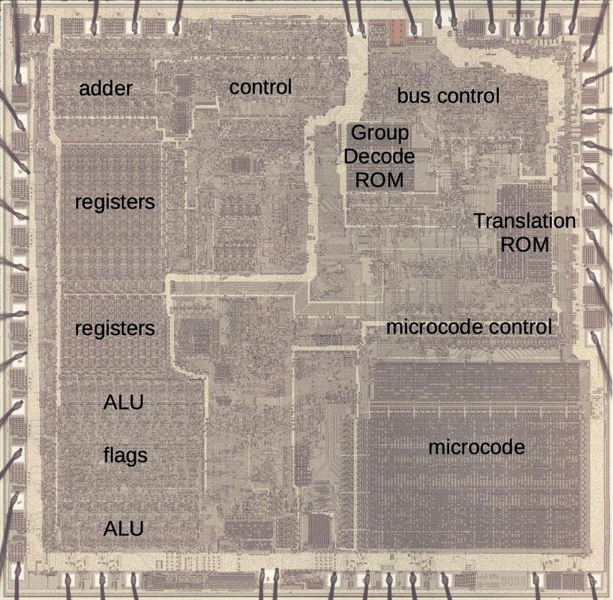
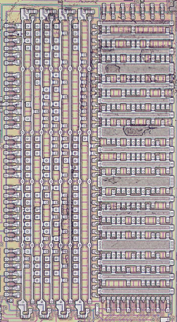
In brief, the microcode in the 8086 consists of 512 micro-instructions, each 21 bits wide. The microcode engine has a 13-bit register that steps through the microcode, along with a 13-bit subroutine register to store the return address for microcode subroutine calls. The microcode engine is assisted by two smaller ROMs: the "Group Decode ROM" to categorize machine instructions, and the "Translation ROM" to branch to microcode subroutines for address calculation and other roles. Physically, the microcode is stored in a 128×84 array. It has a special address decoder that optimizes the storage. The microcode circuitry is visible in the die photo below.
What is microcode?
Machine instructions are generally considered the basic steps that a computer performs. However, each instruction usually requires multiple operations inside the processor. For instance, an ADD instruction may involve computing the memory address, accessing the value, moving the value to the Arithmetic-Logic Unit (ALU), computing the sum, and storing the result in a register. One of the hardest parts of computer design is creating the control logic that signals the appropriate parts of the processor for each step of an instruction. The straightforward approach is to build a circuit from flip-flops and gates that moves through the various steps and generates the control signals. However, this circuitry is complicated and error-prone.
In 1951, Maurice Wilkes came up with the idea of microcode: instead of building the control circuitry from complex logic gates, the control logic could be replaced with another layer of code (i. e. microcode) stored in a special memory called a control store. To execute a machine instruction, the computer internally executes several simpler micro-instructions, specified by the microcode. In other words, microcode forms another layer between the machine instructions and the hardware. The main advantage of microcode is that it turns the processor's control logic into a programming task instead of a difficult logic design task. Microcode also permits complex instructions and a large instruction set to be implemented without making the processor more complex (apart from the size of the microcode). Finally, it is generally easier to fix a bug in microcode than in circuit logic.
Early computers didn't use microcode, largely due to the lack of good storage technologies to hold the microcode. This changed in the 1960s; for example IBM made extensive use of microcode in the System/360 (1964). (I've written about that here.) But early microprocessors didn't use microcode, returning to hard-coded control logic with logic gates.3 This logic was generally more compact and ran faster than microcode, since the circuitry could be optimized. Since space was at a premium in early microprocessors and the instruction sets were relatively simple, this tradeoff made sense. But as microprocessor instruction sets became complex and transistors became cheaper, microcode became appealing. This led to the use of microcode in the Intel 8086 (1978) and 8088 (1979) and Motorola 68000 (1979), for instance.2
The 8086's microcode
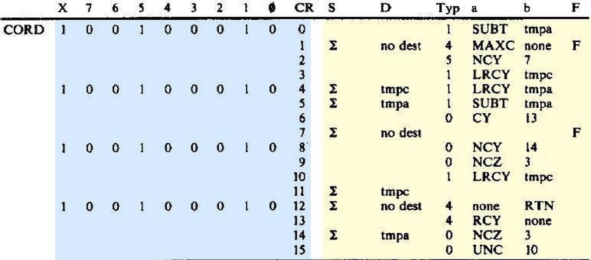
The 8086's microcode is much simpler than in most processors, but it's still fairly complex. The code below is the microcode routine from the 8086 for a routine called "CORD", part of integer division, consisting of 16 micro-instructions. I'm not going to explain how this microcode works in detail, but I want to give a flavor of it. Each line has an address on the left (blue) and the micro-instruction on the right (yellow), specifying the low-level actions during one time step (i.e. clock cycle). Each micro-instruction performs a move, transferring data from a source register (S) to a destination register (D). (The source Σ indicates the ALU output.) For parallelism, the micro-instruction performs an operation or two at the same time as the move. This operation is specified by the "a" and "b" fields; their meanings depend on the type field. For instance, type 1 indicates an ALU instruction such as subtract (SUBT) or left-rotate through carry (LRCY). Type 4 selects two general operations such as "RTN" which returns from a microcode subroutine. Type 0 indicates a jump operation; "UNC 10" is an unconditional jump to line 10 while "CY 13" jumps to line 13 if the carry flag is set. Finally, the "F" field indicates if the condition code flags should be updated. The key points are that the micro-instructions are simple and execute in one clock cycle, they can perform multiple operations in parallel to maximize performance, and they include control-flow operations such as conditional jumps and subroutines.
Each instruction is stored at a 13-bit address (blue) which consists of 9 bits shown explicitly and a 4-bit sequence counter "CR". The eight numbered address bits usually correspond to the machine instruction's opcode. The "X" bit is an extra bit to provide more address space for code that is not directly tied to a machine instruction, such as reset and interrupt code, address computation, and the multiply/divide algorithms.
A micro-instruction is encoded into 21 bits as shown below. Every micro-instruction contains a move from a source register to a destination register, each specified with 5 bits. The meaning of the remaining bits is a bit tricky since it depends on the type field, which is two or three bits long. The "short jump" (type 0) is a conditional jump within the current block of 16 micro-instructions. The ALU operation (type 1) sets up the arithmetic-logic unit to perform an operation. Bookkeeping operations (type 4) are anything from flushing the prefetch queue to ending the current instruction. A memory read or write is type 6. A "long jump" (type 5) is a conditional jump to any of 16 fixed microcode locations (specified in an external table). Finally, a "long call" (type 7) is a conditional subroutine call to one of 16 locations (different from the jump targets).
This "vertical" microcode format reduces the storage required for the microcode by encoding control signals into various fields. However, it requires some decoding logic to process the fields and generate the low-level control signals. Surprisingly, there's no specific "microcode decoder" circuit. Instead, the logic is scattered across the chip, looking for various microcode bit patterns to generate control signals where they are needed.
How instructions map onto the ROM
One interesting issue is how the micro-instructions are organized in the ROM, and how the right micro-instructions are executed for a particular machine instruction. The 8086 uses a clever mapping from the machine instruction to a microcode address that allows machine instructions to share microcode.
Different processors use a variety of approaches to microcode organization. One technique is for each micro-instruction to contain a field with the address of the next micro-instruction. This provides complete flexibility for the arrangement of micro-instructions, but requires a field to hold the address, increasing the number of bits in each micro-instruction. A common alternative is to execute micro-instructions sequentially, with a micro-program-counter stepping through each micro-address unless there is an explicit jump to a new address. This approach avoids the cost of an address field in each instruction, but requires a program counter with an incrementer, increasing the hardware complexity.
The 8086 uses a hybrid approach. A 4-bit program counter steps through the bottom 4 bits of the address, so up to 16 micro-instructions can be executed in sequence without a jump. This approach has the advantage of requiring a smaller 4-bit incrementer for the program counter, rather than a 13-bit incrementer. The microcode engine provides a "short jump" operation that makes it easy to jump within the group of 16 instructions using a 4-bit jump target, rather than a full 13-bit address.
Another important design decision in microcode is how to determine the starting micro-address for each machine instruction. In other words, if you want to do an ADD, where does the microcode for ADD start? One approach is a table of starting addresses: the system looks in the table to find the starting address for ADD, but this requires a large table of 256 entries. A second approach is to use the opcode code value as the starting address. That is, an ADD instruction 0x05 would start at micro-address 5. This approach has two problems. First, you can't run the microcode sequentially since consecutive micro-instructions belong to different machine instructions. Moreover, you can't share microcode since each instruction has a different address in the microcode ROM.
The 8086 solves these problems in two ways. First, the machine instructions are spaced sixteen slots apart in the microcode. In other words, the opcode is multiplied by 16 (has four zeros appended) to form the starting address in the microcode ROM, so there is plenty of space to implement each machine instruction. The second technique is that the ROM's addressing is partially decoded rather than fully decoded, so multiple micro-addresses can correspond to the same physical storage.4
To make this concrete, consider the 8086's arithmetic-logic instructions: one-byte add register to memory, one-byte add memory to register, one-word subtract memory from register, one-word xor register to memory, and so forth. There are 8 ALU operations and each can be byte- or word-sized, with memory as source or destination. This yields 32 different machine opcodes. These opcodes were carefully assigned, so they all have the format 00xxx0xx. The ROM address decoder is designed to look for three 0 bits in those positions, and ignore the other bits, so it will match that pattern. The result is that all 32 of these ALU instructions activate the same ROM column select line, and thus they all share the same microcode, shrinking the size of the ROM.
The microcode ROM's physical layout
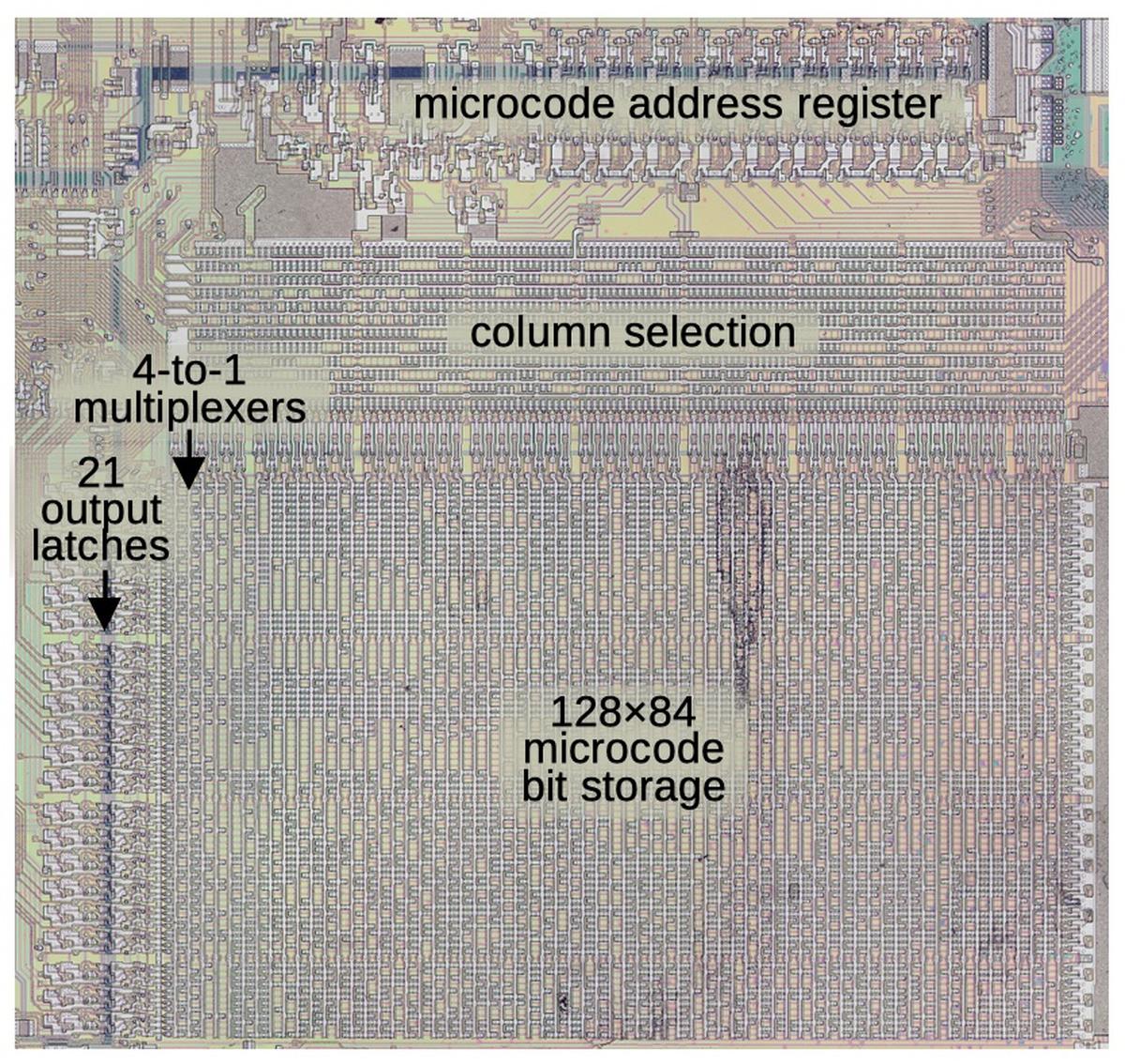
The microcode ROM holds 512 words of 21 bits, so the obvious layout would be 512 columns and 21 rows. However, these dimensions are not practical for physically building the ROM because it would be too long and skinny. Instead, the ROM is constructed by grouping four words in each column, resulting in 128 columns of 84 rows, much closer to square. Not only does this make the physical layout more convenient, but it also reduces the number of column decoders from 512 to 128, reducing the circuitry size. Although the ROM now requires 21 multiplexers to select which of the four rows corresponds to each output bit, the circuitry is still much smaller. There is a tradeoff with the ability to merge addresses together by ignoring bits, though. Each decoder now selects a column of four words, rather than a single word, so each block of four words must have consecutive addresses.
The image above shows how microcode is stored and accessed. At the top is the 13-bit microcode address register, which will be discussed in detail below. The column selection circuit decodes 11 of the 13 address bits to select one column of the microcode storage. At the left, multiplexers select one bit out of each four rows using the two remaining address bits (specifically, the two lowest sequence bits). The selected 21 microcode outputs are latched and fed to the rest of the processor, where they are decoded as described earlier and control the processor's actions.
Optimizing the microcode
In 1978, the number of bits that could be stored in the microcode ROM was rather limited. In particular, the 8086 holds only 512 micro-instructions. Since it has approximately 256 machine-code instructions in its one-byte opcode, combined with multiple addressing modes, and each instruction requires multiple micro-instructions, compression and optimization were necessary to make the microcode fit.5 The main idea was to move functionality out of the microcode and into discrete logic when it made sense. I'll describe some of the ways they did this.
The 8086 has an arithmetic-logic unit (ALU) that performs operations such as addition and subtraction, as well as logical operations such as AND and XOR. Consider the machine instruction ADD, implemented with a few micro-operations that compute the memory address, fetch data, perform the addition, and store the result. The machine instructions for subtraction, AND, or XOR require identical steps, except that the ALU performs a different operation. In total, the 8086 has eight ALU-based operations that are identical except for the operation performed by the ALU.6 The 8086 uses a "trick" where these eight machine instructions share the same microcode. Specifically, the microcode tells the ALU to perform a special operation XI, which indicates that the ALU should look at the appropriate bits of the instruction and do the appropriate operation.7 This shrinks the microcode for these operations by a factor of eight, at the cost of requiring additional logic for the ALU. In particular, the ALU control circuitry has a register to hold the relevant instruction bits, and a PLA to decode these bits into low-level ALU control signals.
Similarly, the 8086 has eight machine instructions to increment a specific register (out of a set of 8), and eight instructions to decrement a register. All 16 instructions are handled by the same set of micro-instructions and the ALU does the increment or decrement as appropriate. Moreover, the register control circuitry determines which register is specified by the instruction, without involvement from the microcode.
Another optimization is that the 8086 has many machine instructions in pairs: an 8-bit version and a 16-bit version. One approach would be to have separate microcode for the two instructions, one to handle a single byte and one to handle two bytes. Instead, the machine instructions share microcode. The complexity is moved to the circuitry that moves data on the bus: it looks at the low bit of the instruction to determine if it should process a byte or a word. This cuts the microcode size in half for the many affected instructions.
Finally, simple instructions that can take place in one cycle are implemented with logic gates, rather than through microcode. For instance, the CLC (clear carry flag) instruction updates the flag directly. Similarly, prefix instructions for segment selection, instruction locking, or repetition are performed in logic. These instructions don't use any microcode at all, which will be important later below.
Using techniques such as these, about 75 different instruction types are implemented in the microcode (instead of about 256), making the microcode much smaller. The tradeoff is that the 8086 requires more logic circuitry, but the designers found the tradeoff to be worthwhile.
The ModR/M byte
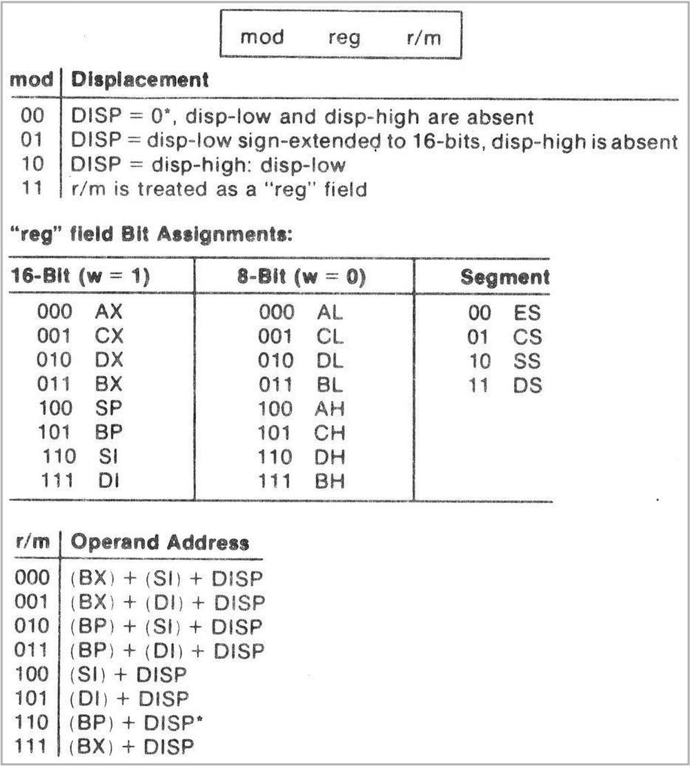
There's another complication for 8086 microcode, however. Most 8086 instructions have a second byte: the ModR/M byte, which controls the addressing mode for the instructions in a complex way (shown below). This byte gives 8086 instructions a lot of flexibility: you can use two registers, a register and a memory location, or a register and an "immediate" value specified in the instruction. The memory location can be specified by 8 index register combinations with a one-byte or two-byte displacement optionally added. (This is useful for accessing data in an array or structure, for instance.) Although these addressing modes are powerful, they pose a problem for the microcode.
These different addressing modes need to be implemented in microcode, since different addressing modes require different sequences of steps. In other words, you can't use the previous trick of pushing the problem into logic gates. And you clearly don't want a separate implementation of each instruction for each addressing mode since the size of the microcode would multiply out of control.
The solution is to use a subroutine (in microcode) to compute the memory address. Thus, instructions can share the microcode for each addressing mode. This adds a lot of complexity to the microcode engine, however, since it needs to store the micro-address for a micro-subroutine-call so it can return to the right location. To support this, the microcode engine has a register to hold this return address. (Since it doesn't have a full stack, you can't perform nested subroutine calls, but this isn't a significant limitation.)
The microcode ends up having about 10 subroutines for the different addressing modes, as well as four routines for the different sizes of displacement. (The 8 possibilities for source registers are handled in the register selection logic, rather than microcode.) Thus, the microcode handles the 256 different addressing modes with about 14 short routines that add the appropriate address register(s) and the displacement to obtain the memory address.
One more complication is that machine instructions can switch the source and destination specified by the ModR/M byte, depending on the opcode. For example, one subtract instruction will subtract a memory location from a register, while a different subtract instruction subtracts a register from a memory location. The two variants are distinguished by bit 1 of the instruction, the "direction" bit. These variants are handled by the control logic, so the microcode can ignore them. Specifically, before the source and destination specifications go to the register control circuitry, a crossover circuit can swap them based on the value of the direction bit.
The Translation ROM
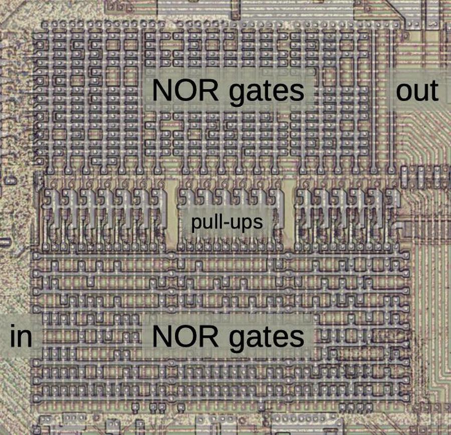
As explained above, the starting address for a machine instruction is derived directly from the instruction's opcode. However, the microcode engine needs a mechanism to provide the address for jump and call operations. In the 8086, this address is hard-coded into the Translation ROM, which provides a 13-bit address.8 It holds ten destination addresses for jump operations and ten (different) addresses for call operations.
A second role of the Translation ROM is to hold target addresses for each ModR/M addressing mode, pointing to the code to compute the effective address. As a complication, two of the jump table entries in the Translation ROM are implemented with conditional logic, depending on whether or not the instruction's memory address calculation includes a displacement. By wiring this condition into the Translation ROM, the microcode avoids the need to test this condition.
The image below shows how the Translation ROM appears on the die. It is implemented as a partially-decoded ROM with multiplexed inputs.9 The inputs are at the bottom left. For a jump or call, the ROM uses 4 input bits from the microcode output, since the microcode selects the jump targets. For an address computation, it takes 5 bits from the instruction's ModR/M byte, so the routine is selected by the instruction. The ROM has additional input bits to select the mode (jump, call, or address) and for the conditional jumps. The decoding logic (left half) activates a row in the right half, generating the output address. This address exits at the bottom and is loaded into the micro-address register below the Translation ROM.
The Group Decode ROM
In the discussion above, I've discussed how various categories of instructions are optimized. For instance, many instructions have a bit that selects if they act on a byte or a word. Many instructions have a bit to reverse the direction of the operation's memory and register accesses. These features are implemented in logic rather than microcode. Other instructions are implemented outside microcode entirely. How does the 8086 determine which way to process an instruction?
The Group Decode ROM takes an instruction opcode and generate 15 signals that indicate various categories of instructions that are handled differently.10 The outputs from the Group Decode ROM are used by various logic circuits to determine how to handle the instruction. Some cases affect the microcode, for instance calling a microcode addressing routine if the instruction has a ModR/M byte. In other cases, these signals act "downstream" of the microcode, for example to determine if the operation should act on a byte or a word. Other signals cause the microcode to be bypassed completely.
Specially-encoded instructions
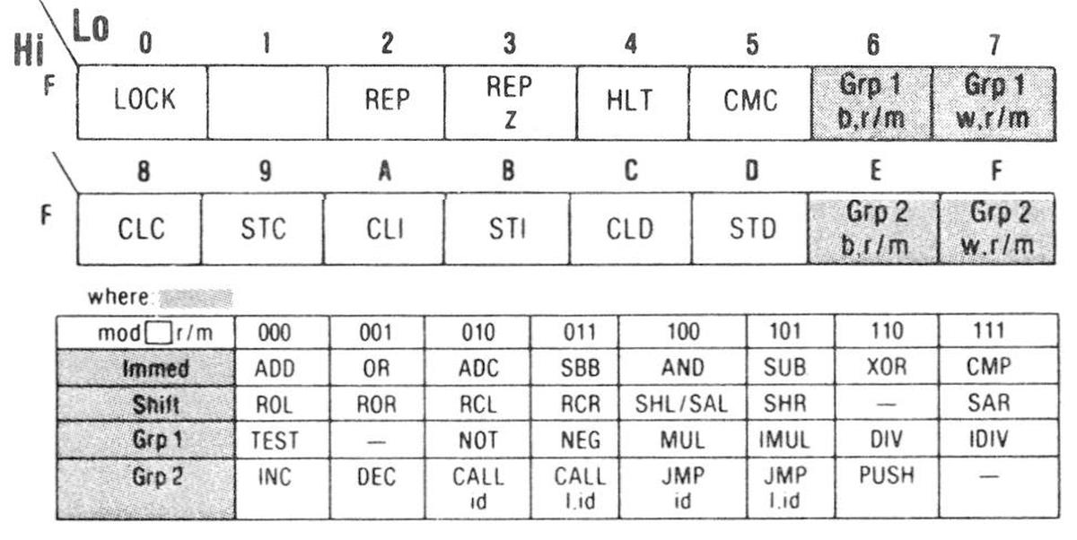
For most of the 8086 instructions, the first byte specifies the instruction. However, the 8086 has a few instructions where the ModR/M byte completely changes the meaning of the first byte. For instance, opcode 0xF6 (Grp 1 below) can be a TEST, NOT, NEG, MUL, IMUL, DIV, or IDIV instruction based on the value of the ModR/M byte. Similarly, opcode 0xFE (Grp 2) indicates an INC, DEC, CALL, JMP, or PUSH instruction.11
This encoding may seem a bit random, but there's a reason behind it. Most instructions act on a source and a destination. But some, such as INC (increment) use the same register or memory location for the source and the destination. Others, such as CALL or JMP, only use one address. Thus, the "reg" field in the ModR/M byte is redundant. Since these bits would be otherwise "wasted", they are used instead to specify different instructions. (There are only 256 single-byte opcodes, so you want to make the best use of them.)
The implementation of these instructions in microcode is interesting. Since the instructions share the same first byte, the standard microcode mapping would put them at the same microcode address. However, these instructions are treated specially, with the "reg" field from the ModR/M byte copied into the lower bits of the microcode address. In effect, the instructions are treated as opcodes 0xF0 through 0xFF, so the different instruction variants execute at separate microcode addresses. You might expect a collision with the opcodes that really have the values 0xF0 through 0xFF. However, the 8086 opcodes were cleverly arranged so none of the other instructions in this range use microcode. As you can see above, the other instructions are prefixes (LOCK, REP, REPZ), halt (HLT), or flag operations (CMC, CLC, STC, CLI, STI, CLD, STD), all implemented outside microcode. Thus, the range 0xF0-0xFF is freed up for the "expanded" instructions.
The hardware implementation for this is not too complex. The Group ROM produces an output for these special instructions. This causes the microcode address register to load the appropriate bits from the ModR/M byte, causing the appropriate microcode routine to be executed.
The microcode address register
The heart of the microcode engine is the microcode address register, which determines which microcode address to execute. As described earlier, the microcode address is 13 bits, of which 8 bits generally correspond to the instruction opcode, one bit is an extra "X" instruction bit, and 4 bits are sequentially incremented. The diagram below shows how the circuitry for the bits is arranged. The 9 instruction bits each have a nearly-identical circuit. The sequence bits have more circuitry and each one is different, because the circuit to increment the address is different for each bit.
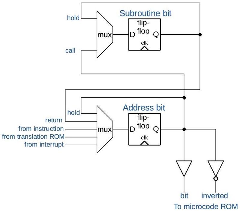
The schematic below shows the circuitry for one bit in the microcode address register. It has two flip-flops: one to hold the current address bit and one to hold the old address while performing a subroutine call. A multiplexer (mux) selects the input to each flip-flop. For instance, if the microcode is waiting for a memory access, the "hold" input to the multiplexer causes the current address to loop around and get reloaded into the flip-flop. For a subroutine call, the "call" input saves the current address in the subroutine flip-flop. Conversely, when returning from a subroutine, the "return" input loads the old address from the subroutine flip-flop. The address flip-flop also has inputs to load the instruction as the address, to load an address from the translation ROM, or to load an interrupt microcode handler address. The circuit sends the address bit (and inverted address bit) to the microcode ROM's address decoder.
Each bit has some special-case handling, so this schematic should be viewed as an illustration, not an accurate wiring diagram. In particular, the sequence bits also have inputs from the incrementer, so they can step to the next address. The low-order bits have instruction inputs to handle the specially-encoded "group" instructions discussed in the previous section.
The control signals for the multiplexers are generated from various sources. A circuit called the loader starts processing of an instruction, synchronized to the prefetch queue and instruction fetch from memory. The call and return operations are microcode instructions. The Group Decode ROM controls some of the inputs, for instance to process a ModR/M byte. Thus, there is a moderate amount of conditional logic that determines the microcode address and thus what microcode gets executed.
Conclusions
This has been a lot of material, so thank you for sticking with it to the end. I draw three conclusions from studying the microcode engine of the 8086. First, the implementation of microcode is considerably more complex than the clean description of microcode that is presented in books. A lot of functionality is implemented in logic outside of microcode, so it's not a "pure" microcode implementation. Moreover, there are many optimizations and corner cases. The microcode engine has two supporting ROMs: the Translation ROM and the Group Decode ROM. Even the microcode address register has complications.
Second, the need for all these optimizations shows how the 8086 was just on the edge of what was practical. The designers clearly went to a lot of effort to get the microcode to fit in the space available.
Finally, looking at the 8086 in detail shows how complex its instruction set is. I knew in the abstract that it was much more convoluted than, say, an ARM chip. But seeing all the special case circuitry on the die to handle the corner cases of the instruction set really makes this clear.
I plan to continue reverse-engineering the 8086 die so follow me on Twitter @kenshirriff or RSS for updates. I've also started experimenting with Mastodon recently as @[email protected]. If you're interested in the 8086, I wrote about the 8086 die, its die shrink process and the 8086 registers earlier.
Notes and references
-
The 8086 microcode was disassembled (link) a couple of years ago by Andrew Jenner by extracting the bits from my die photos. My post here is a bit different, looking at hardware that runs the microcode, rather than the contents of the microcode. ↩
-
According to Wikipedia, the Zilog Z8000 (1979) didn't use microcode, which is a bit surprising for that timeframe. This design decision had the advantage of reducing transistor count, but the disadvantage of hard-to-fix logic bugs in the instruction decoder. ↩
-
As an example of a non-microcoded processor, the MOS 6502 (1975) used a PLA (Programmable Logic Array) to perform much of the decoding (details). A PLA provides a structured way of implementing logic gates in a relatively dense array. A PLA is kind of like a ROM—a PLA can implement a ROM and vice versa—so it can be hard to see the difference. The usual distinction is that only one row of a ROM is active at a time, the address that you're reading out. A PLA is more general since multiple rows can be active at a time, combined to form the outputs.
The Z80 had a slightly different implementation. It used a smaller PLA to perform basic decoding of instructions into various types. It then generated control signals through a large amount of "random" logic (so-called because of its appearance, not because it's actually random). This logic combined instruction types and timing signals to generate the appropriate control signals. ↩
-
In a "normal" ROM, the address bits are decoded with logic gates so each unique address selects a different storage column in the ROM. However, parts of the decoder circuitry can "ignore" bits so multiple addresses select the same storage column. For a hypothetical example, suppose you're decoding 5-bit addresses. Instead of decoding 11010 and 11011 separately, you could ignore the last bit so both addresses access the same ROM data. or you could ignore the last three bits so all 8 addresses of the form 11xxx go to the same ROM location (where x indicates a bit that can be either 0 or 1). This makes the ROM more like a PLA (Programmable Logic Array), but still accessing a single row at a time. ↩
-
The Intel 8087 was the floating point co-processor for the 8086. The 8087 required a lot of microcode, more than could fit in a standard ROM on the die. To get the microcode to fit, Intel created a special ROM that stored two bits per transistor (instead of one) by using four different sizes of transistors to generate four different voltages. Analog circuitry converted each voltage level into two bits. This complex technique doubled the density (at least in theory), allowing the microcode to fit on the chip. I wrote about the 8087's non-binary ROM here. ↩
-
The ALU operations that are grouped together are add, add with carry, subtract, subtract with borrow, logical AND, logical XOR, logical OR, and compare. The compare operation may seem out of place in this list, but it is implemented as a subtract operation that updates the condition flags without changing the value. Operations such as increment, decrement, negation, and logical NOT may seem like they should be included, but since they operate on a single argument instead of two, they are implemented differently at the microcode level. Increment and decrement are combined in the microcode, however. Negation and logical NOT could be combined except that negation affects the condition code flags, while NOT doesn't, so they need separate microcode. (This illustrates how subtle features of the instruction set can have more impact than you might expect.) Since the ALU doesn't have hardware multiplication and division, the multiplication and division operations are implemented separately in microcode with loops. ↩
-
The ALU itself isn't examining instruction bits to decide what to do. There's some control circuitry next to the ALU that uses a PLA (Programmable Logic Array) to examine the instruction bits and the microcode's ALU command to generate low-level control signals for the ALU. These signals control things such as carry propagation, argument negation, and logical operation selection to cause the ALU to perform the desired operation. ↩
-
The Translation ROM has one additional output: a wire indicating an address mode that uses the BP register. This output goes to the segment register selection circuitry and selects a different segment register. The reason is that the 8086 uses the Data Segment by default for effective address computation, unless the address mode uses BP as a base register. In that case, the Stack Segment is used. This is an example of how the 8086 architecture is not orthogonal and has lots of corner cases. ↩
-
You can also view the Translation ROM as a PLA (Programmable Logic Array) constructed from two layers of NOR gates. The conditional entries make it seem more like a PLA than a ROM. Technically, it can be considered a ROM since a single row is active at a time. I'm using the name "Translation ROM" because that's what Intel calls it in the patents. ↩
-
Although the Group Decode ROM is called a ROM in the patent, I'd consider it more of a PLA (programmable logic array). Conceptually it holds 256 words, one for each instruction. But its implementation is an array of logic functions. ↩
-
These instructions were called "Group 1" and "Group 2" instructions in the 8086 documentation. Later Intel documentation renamed them as "Unary Group 3", "INC/DEC Group 4" and "Indirect Group 5". Some details are here. The 8086 has two other groups of instructions where the reg field defines the instruction: the "Immediate" instructions 0x80-0x83 and the "Shift" instructions 0xD0-0xD3. For these opcodes, the different instructions were implemented by the ALU. As far as the microcode was concerned, these were "normal" instructions so I won't discuss them in this post.
I should mention that although the 8086 opcodes are always expressed in hexadecimal, the encoding makes much more sense if you look at it in octal. Details here. The octal encoding also applies to other related chips including the 8008, 8080, and Z80. ↩


18 comments:
In describing the ROM size you have "48" in a couple of places instead of "84".
Thanks, Malcolm. I've fixed that.
In my first microprocessor class in the late 70s, we studied the 8080. The instructions were only defined in octal, there were a lot of 3-bit fields that made sense when you hand assembled instructions. We had a microprocessor trainer we could take home for hardware stuff, while we ran our software in an emulator running on an IBM mainframe submitted on punch cards.
Being aggressive and chauvinistic against over 130 million people just so you can virtue signal to the world how morally superior you are... that speaks volumes of you. Absolutely disgusted with you and your choices. And with the hypocrisy... several wars around, children killed by US, and you say nothing about it. Just disgusting. I am not much, but you lost me forever. But most important, you lost any moral compass you may have had. And that, that is a problem.
BTW, I am not russian, and I don't support the Ukraine invasion. I am just someone that doesnt support racism and collective punishment. And biggots. So, I will stay away from you.
Thanks again, Ken!
I mean, it's no tube-based de-bouncer circuit but it's still cool, I guess... ;-p
Interesting, though mostly over my head. I'm curious about the requirements that led Intel engineers to implement such a complicated ISA. Any links? The Wikipedia article (https://en.wikipedia.org/wiki/Intel_8086) is light on details.
Interesting you mention the lack of microcode for Zilog Z8000.
The lack of microcode (I think 18k transistors, probably the lowest transistor count of all the 16bit micros) made a radiation hardening a lot easier than others and the chip found a niche in military systems due to it's ability to do 32 bit and 64 bit maths and on a clock for clock basis competitive performance against the 68K.
Apparently Shinta who implemented the design had a lot of trouble fighting bugs due the complicated decoder and there is an IEEE article he wrote about it that I know about but is pay walled and have never read:
https://www.sciencedirect.com/science/article/abs/pii/0142694X81900065?utm_source=pocket_mylist
According to the computer history interview on the Z8k design (lost the link) the initial plan for was an introduction in 1978 at the same time as the 8086 but was delayed to 1979 just before the 68k. Searching usenet people were still complaining about the first issues with the chip but also about Zilog being a small company and not getting support.
The Zilog Z8000 deserves more attention. It was a direct competitor with the 8086 and shared the multiplexed address/data bus and had an upgrade path from the its 8bit forebear via assembly source code translators. It was squeezed out between the 8086 when IBM chose it for the 5150 PC and 68000 which was adopted for high end Unix systems.
https://www.eejournal.com/article/in-memoriam-dr-bernard-peuto-architect-of-zilogs-z8000-and-z8/
"In other words, the opcode is multiplied by 16 (has four zeros appended)" - might read better as "In other words, the opcode is multiplied by 16 (has four zero bits appended)" - Later you use bits in a similar more clear way.
Hi Ken,
Your work is amazing!
I cannot imagine how you did all this analysis without ad-hoc tools (both hardware and software).
Could you comment us the tools/procedures that you use? More.... I think this could be the right topic for some or your geniously posts.
Best regards!
Federico
The 8086/8088 microcode disassemble by Andrew Jenner is well known,
but researching a bit back in time, I found somewhere a 80186 disassembler,
made in pascal.
I have the files, but it seems I cannot find links now.
There are no emails or names in code, the readme file starts:
"!!! IMPORTANT NOTE !!!
There are missing bits in this, due to the quality of the photo used [1],
and other errors as well.
I uploaded this archive because other people might be interested, even in
this raw state, and also I likely won't be spending any more time improving
it.
[1] https://siliconpr0n.org/archive/doku.php?id=mcmaster:amd:80186"
Bleuge, that 80186 disassembly may have come from this thread on the vcfed forum, the same one that reengine announced his microcode disassembly:
https://forum.vcfed.org/index.php?threads/8088-8086-microcode-disassembly.77933/page-2
A different user, dreNorteR, used the same method on the 80186, and got pretty far.
Hi Ken,
This microcode implementation difficulty is indeed head scratching and your investigation skills are just awesome.
I bumped to a very interesting resources on chips details (https://www.oguchi-rd.com) including development papers, analyses and hand made masks design process with detailed notes made available by Mr. Tetsuji Oguchi, apparently the author of many chips himself.
There are detailed die photos of many chips also available on his page. It is interesting to see one of the official(?) 8086 copy by OKI - 80C86A variant from 1985 with various modifications:
https://www.oguchi-rd.com/Accomplishment/Projects/Die%20Photo%20by%20Hugin/80C86A_20x%20Micrograph.pdf
Thank you for sharing your work and explanations,
KR
P
@JRD: yes, you find it! thanks for finding the reference I was looking for.
Incredible.
It's articles like this that I get to know how the magic happens.
And imagine that this "magic" is currently used with more components.
Thanks again for showing us how this works.
Top notch article as always, I hope it will motivate more hobbyists to play with microcode - it is not just for CPUs but complex and fast application specific processors can be implemented (e.g. GPU drawing routines). For one of my projects I wrote 2 microcoded custom processors, one to write to memory by consuming Intel HEX ASCII stream, and the other vice versa. Most of hardware was generated from the microcode itself - https://hackaday.io/project/181664-intel-hex-files-for-fpgas-no-embedded-cpus
Thank you for the very interesting article. You mention that segment overrides are implemented using logic rather than microcode. My question is related to this: one of the "quirks" of the x86 architecture is that the LODSB/LODSW instruction accepts segment override prefixes, but the STOSB/STOSW instruction does not. Do you have an explanation for this?
Thank you! This really deepens my understanding of microcode
Post a Comment