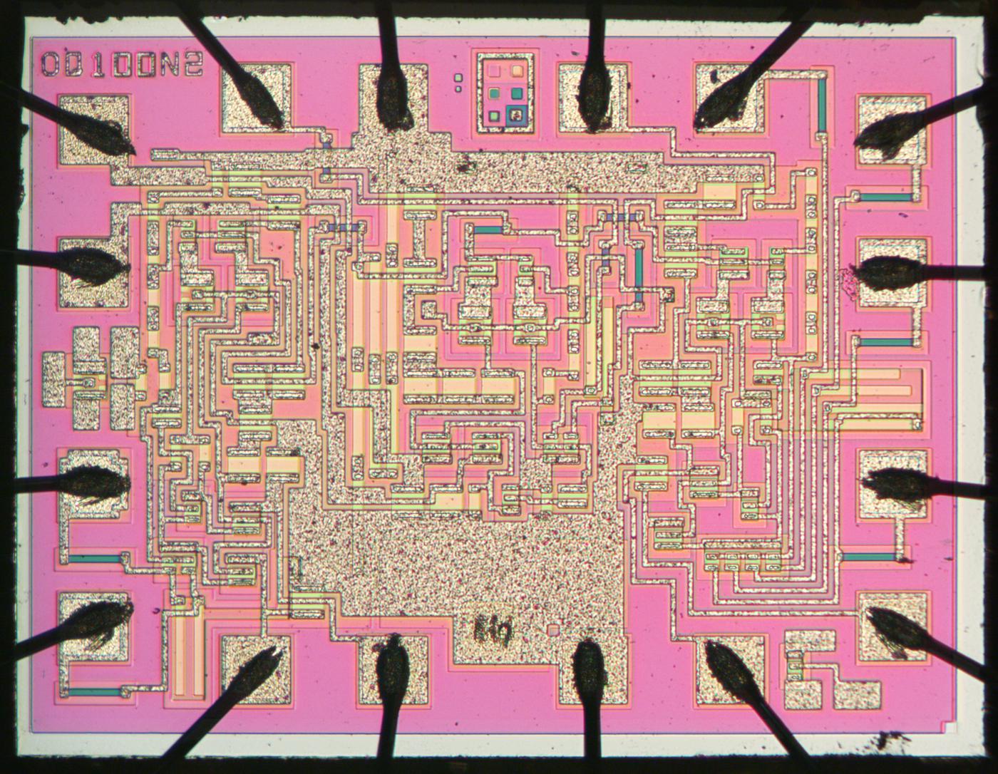
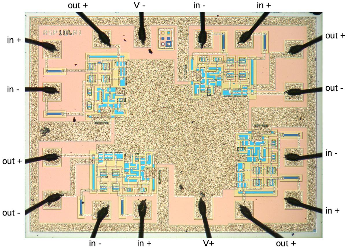
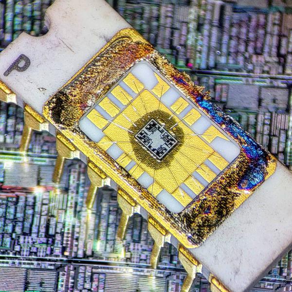
Recently, I received a die photo of a mystery integrated circuit, the OQ100,1 from EvilMonkeyDesignz. I analyzed the die photo and found that it is a logic chip implemented with fast ECL (Emitter-Coupled Logic) circuitry, probably from the early 1970s. The chip contains three logic gates, two with 2 inputs and one with 4 inputs. Each gate has non-inverted and inverted outputs, acting as both an OR gate and a NOR gate. This blog post summarizes my investigation. (I also recently analyzed the OQ104, a different chip in this series.)
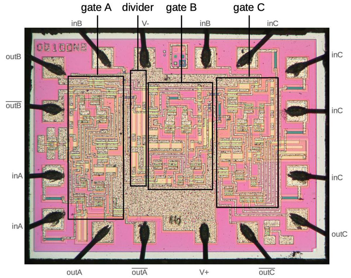
The die photo above shows the chip under the microscope. Most of the silicon appears bright pink in this image. Regions of silicon with different doping appear green or yellowish and form the transistors and resistors of the chip. The speckled regions are the metal layer on top of the silicon, wiring the circuitry together. Around the edges, the black bond wires connect the chip to the external pins.
The chip's components
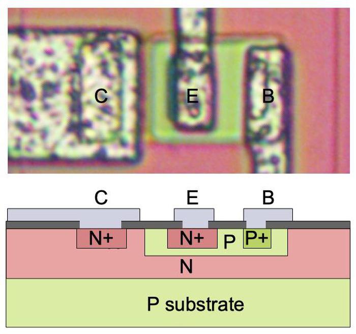
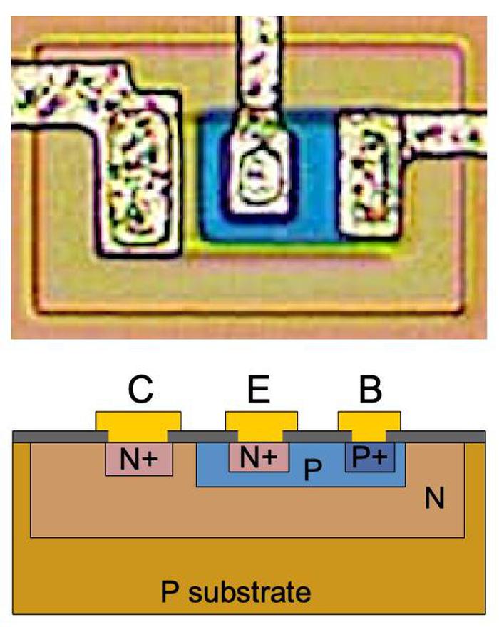
Transistors are the key components in a chip. This chip uses a type of transistor called an NPN transistor. The photo below shows a transistor as it appears on the chip. Underneath the photo is a cross-section drawing showing approximately how the transistor is constructed. The transistor is more complicated than the N-P-N sandwich you see in books, but if you look carefully at the vertical cross-section below the 'E', you can find the N-P-N layers that form the transistor. The emitter (E) wire is connected to N+ silicon. Below that is a P layer connected to the base contact (B). And below that is an N layer connected to the collector (C).
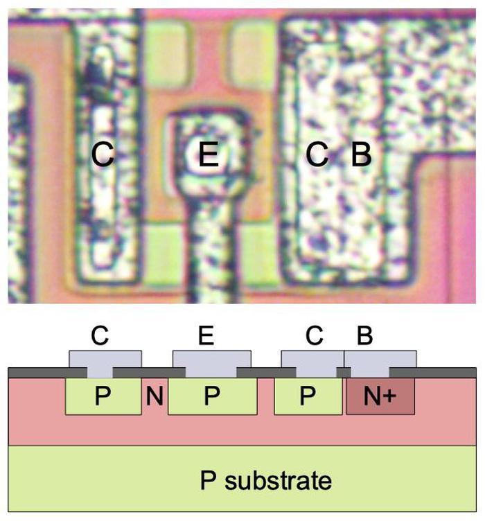
The chip also uses a few PNP transistors. Although you might expect a PNP transistor to simply be the reverse of an NPN transistor, it has a different structure, with the regions arranged laterally instead of vertically. The collector and base form concentric square rings around the emitter. The base wire is not connected to the base region directly. Instead, the wire is at a distance, and the base signal travels underneath through the N layer.
The PNP transistors in this chip have another complication. The collector is split, so the transistor has two collectors. Moreover, one of the collectors is wired directly to the base. In the photo above, you can see how the collector region is split vertically, so there is one collector on the left and one on the right, with collector on the right connected to the base. This construction may seem bizarre, but it is common in integrated circuits. The motivation is to build a current mirror, where both collectors pass the same current.
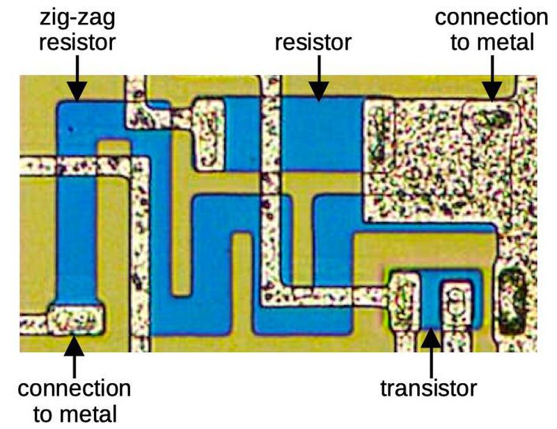
The other key components of this chip are the resistors. The photo below shows two resistors as they appear on the die. The resistors are formed from strips of higher-resistance P silicon, which appears pink in the die photos. Each end of a resistor is connected to the metal layer; the metal in the middle connects the two resistors together in series. (A metal wire also passes over the resistor but is not connected.) A resistor has higher resistance if it is longer and narrower, so these resistors have relatively high resistance.2 Resistors are relatively large on an integrated circuit and fairly inaccurate.
The circuitry
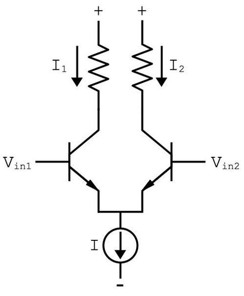
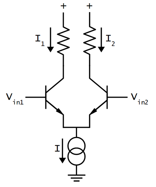
Once the components can be recognized on the die, the circuit can be traced out and reverse-engineered. But before I describe the complete circuit, I'll explain how ECL (Emitter-Coupled Logic) works.3 The schematic below shows a differential pair, or long-tailed pair, which amplifies the difference between its two inputs. (This circuit is also common in analog circuits, forming the heart of an op-amp.) The basic idea is that a current sink (the circle at the bottom) generates a fixed current I. This current gets split between the left path (I1) and the right path (I2). If the transistor on the left has a higher input voltage than the transistor on the right, most of the current will go to the left. But if the transistor on the right has a higher input, most of the current will go to the right. This circuit amplifies the voltage difference: even a small difference between the two inputs will switch most of the current from one side to the other.
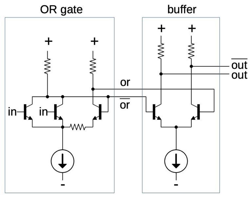
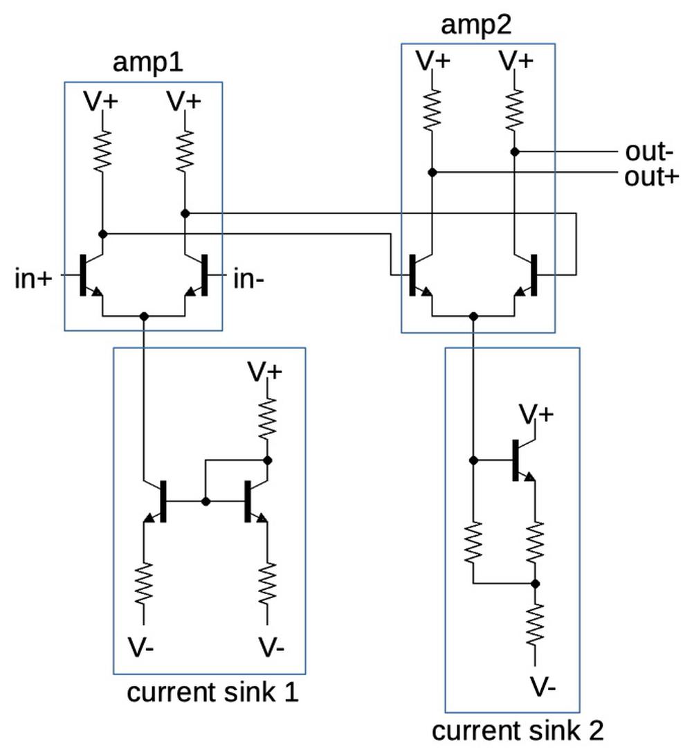
To make this into an OR gate, we can put multiple transistors on the left. If any input is high, the current will be switched to the left, otherwise the current will be switched to the right. Since the current pulls that side low, the left branch will be the NOR output while the right branch will be the OR output. (With ECL, you get both the complemented and uncomplemented outputs "for free".) The schematic below shows how one logic gate is implemented; this is a two-input gate. The gate uses a second differential pair to buffer and amplify the outputs. The current sink circuit is discussed in a footnote.4
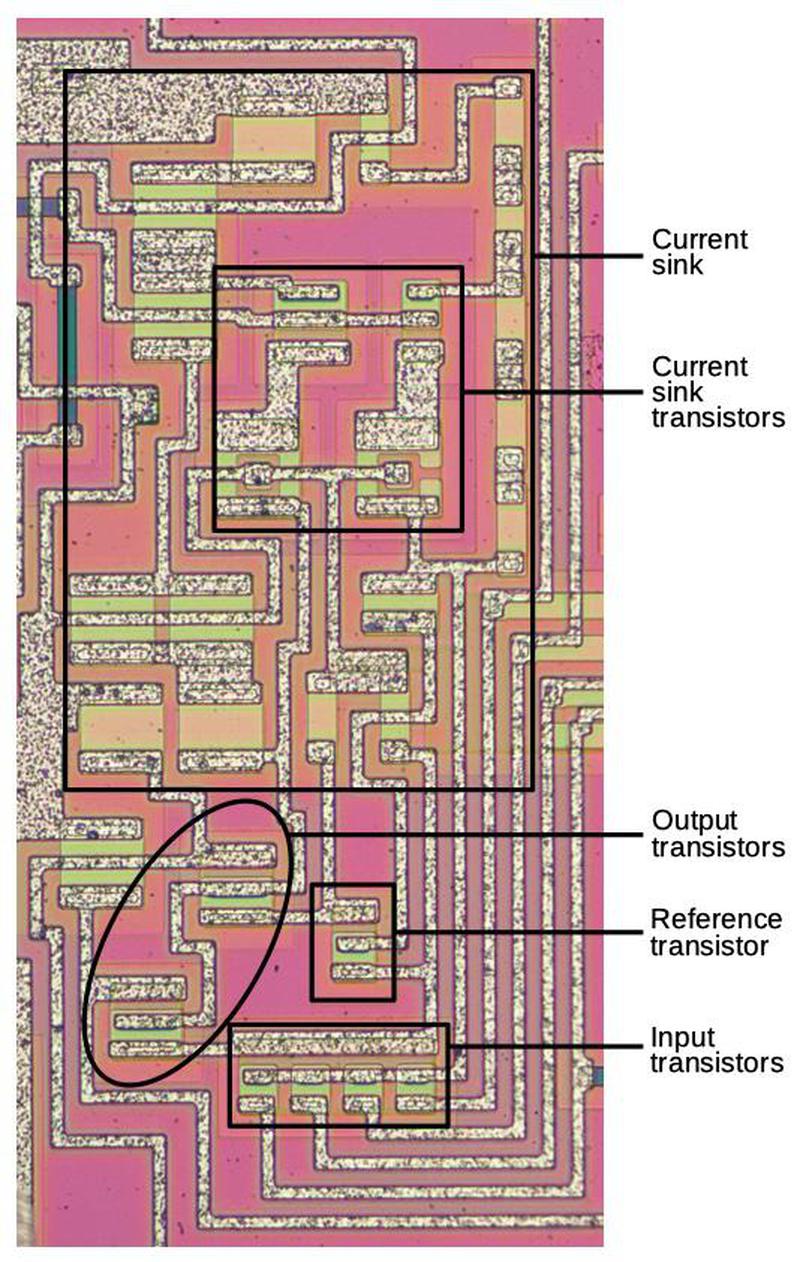
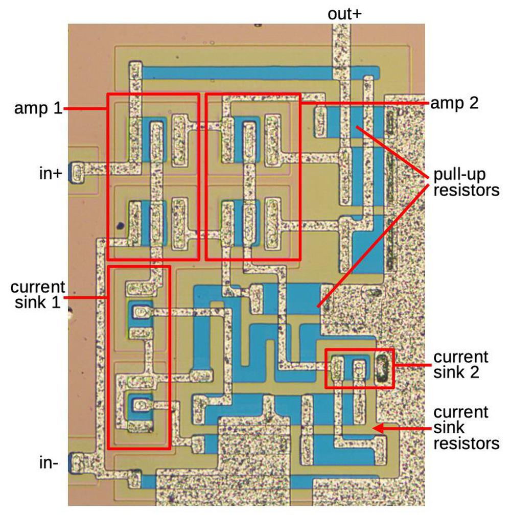
The diagram below shows how the four-input gate is implemented on the die. The majority of the area is occupied by the current sink and the associated resistors. The NPN and PNP transistors are relatively compact, but the resistors occupy a lot of space. At the bottom, the four input transistors implement the OR function, along with the reference transistor on the other branch. The output transistors are larger so they can provide more current.
The diagram below shows how the three gates are arranged on the die. (The gate described above is at the right.) The voltage divider resistors provide a voltage reference for the current sources.
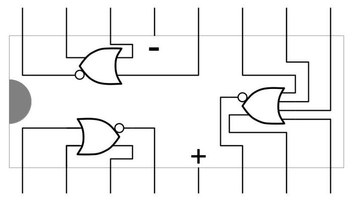
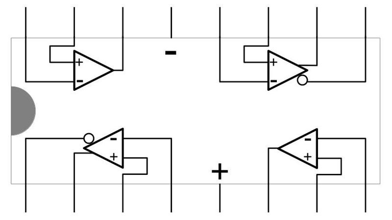
Putting everything together, the diagram below shows how the circuitry of the chip maps onto its 16 pins. The three OR gates are represented by the OR symbols; the gate on the right has four inputs. Each gate has a non-inverted output and an inverted output, which is indicated by a bubble. I don't know what voltages the chip takes, so I've indicated the power pins with + and -.
I announce my latest blog posts on Twitter, so follow me @kenshirriff. Many thanks to EvilMonkeyz Designs for providing the photos; follow on Instagram or Twitter for more interesting die photos.
Notes
-
A reader said that Philips used the OQ designation for their custom integrated circuits. That would explain why I was unable to find these chips in a databook. ↩
-
The resistance of a resistor is proportional to the length divided by the width. To understand this, note that a region twice as long is the same as two resistors in series, so it has twice the resistance. A region twice as wide is the same as two resistors in parallel, so it has half the resistance. ↩
-
The logic circuit on this chip has a couple of differences from standard ECL gates. A typical ECL gate has inputs on one branch and a reference voltage connected to the transistor on the other branch. Thus, an input higher than the reference voltage is a logic 1, and an input lower than the reference voltage in a logic 0. This gate, however, uses the output of the first branch as the input to the second branch. If an input is high, it pulls this output low, shutting off the other branch. Conversely, if the input is low, the output goes high, turning on the other branch.
I'm not sure what the motivation is for this design. It looks a bit like NTL (Non-Threshold Logic), since there isn't a threshold set by a reference voltage. One possibility is that the circuit implements a Schmitt-trigger, a circuit with hysteresis, where once it turns on, the input must drop significantly lower to turn it off.
The second difference between this circuit and a typical ECL gate is the output buffer. ECL gates typically use an emitter follower, rather than a second differential pair. ↩
-
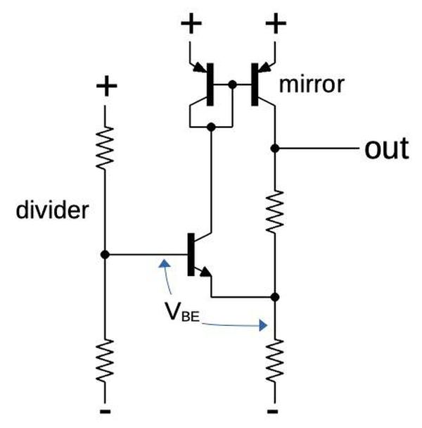
I'll just briefly describe the current sink circuit, shown below. Two large resistors form a voltage divider that produces a reference voltage midway between the two supply voltages (maybe 0 volts). Due to the behavior of transistors, VBE will be one diode drop (~0.7 V). The rest of the circuit generates the "correct" current through the lower-right resistor to achieve this voltage drop. On the chip, the two PNP transistors at the top are one transistor with two collectors. They implement a current mirror, where the current through the right transistor matches the current through the left transistor.
The current sink circuit used in the chip. The divider is shared by all the current sinks on the chip.
