How the 8086 processor's microcode engine works

The 8086 microprocessor was a groundbreaking processor introduced by Intel in 1978. It led to the x86 architecture that still dominates desktop and server computing. The 8086 chip uses microcode internally to implement its instruction set. I've been reverse-engineering the 8086 from die photos and this blog post discusses how the chip's microcode engine operated. I'm not going to discuss the contents of the microcode1 or how the microcode controls the rest of the processor here. Instead, I'll look at how the 8086 decides what microcode to run, steps through the microcode, handles jumps and calls inside the microcode, and physically stores the microcode. It was a challenge to fit the microcode onto the chip with 1978 technology, so Intel used many optimization techniques to reduce the size of the microcode.

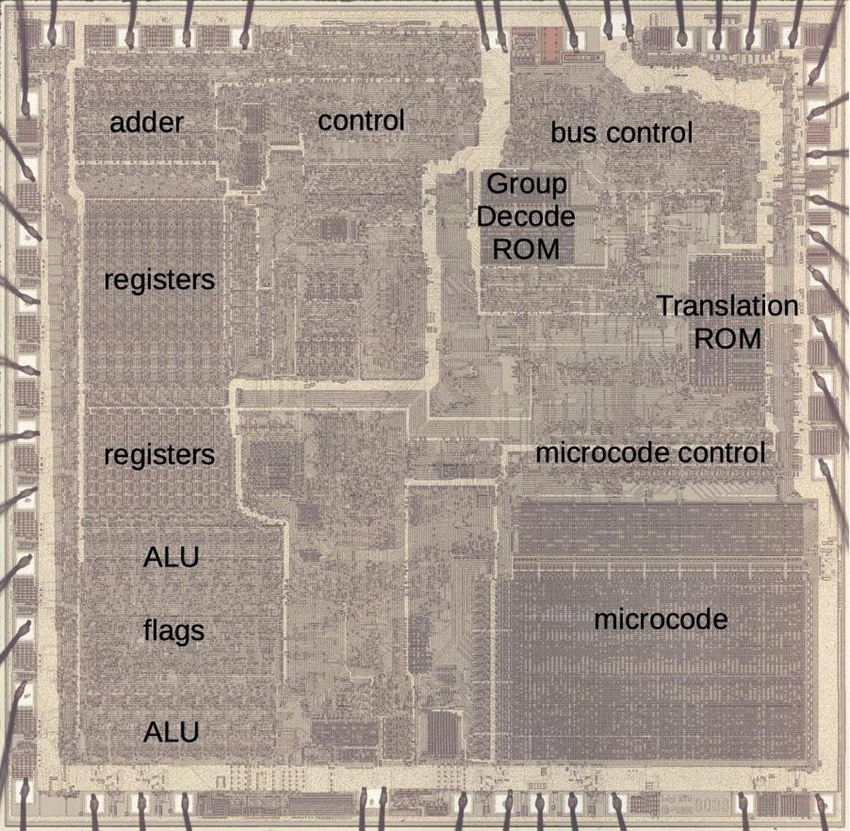
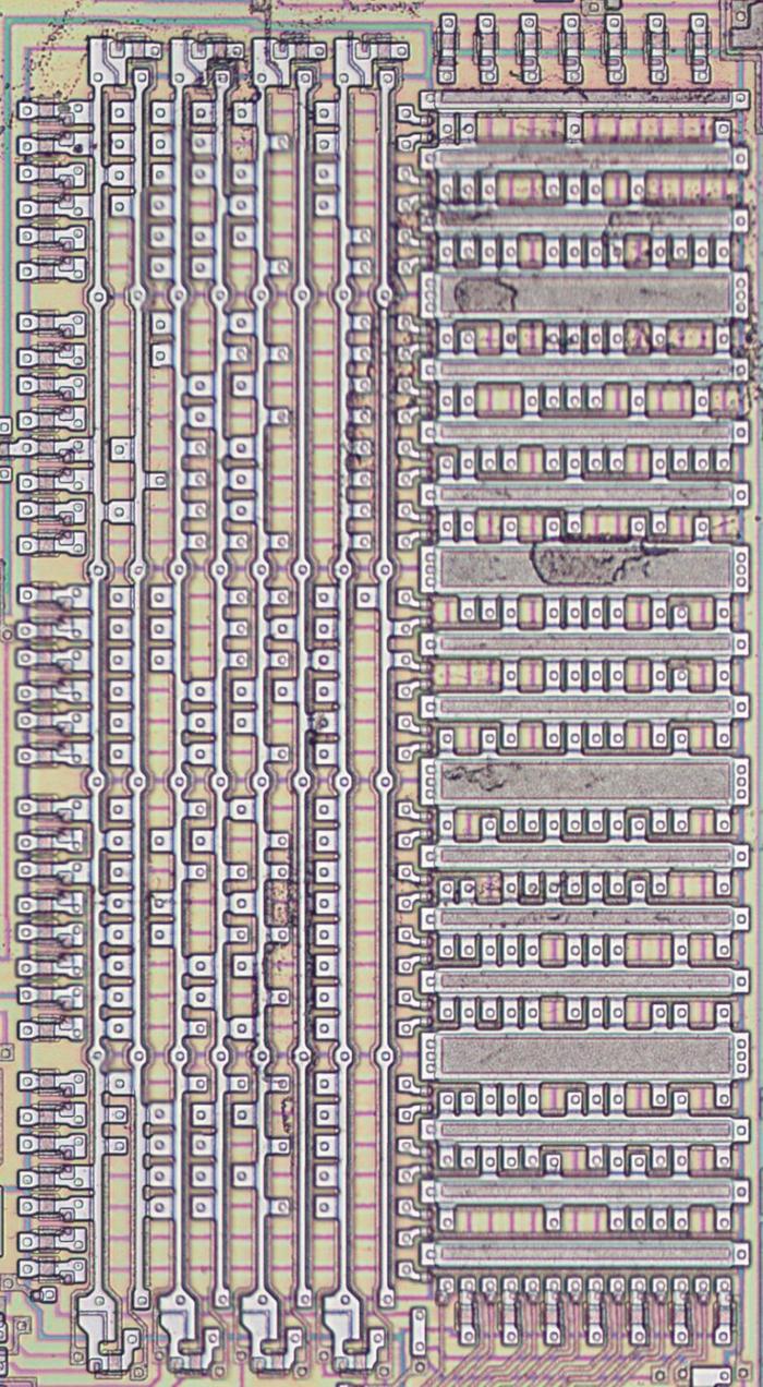
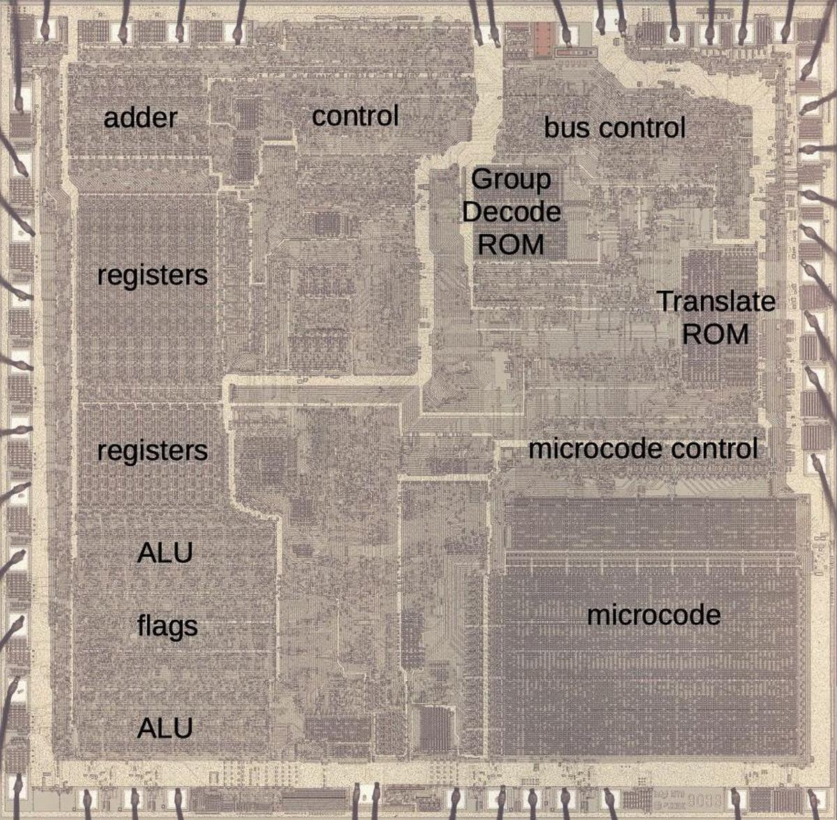
In brief, the microcode in the 8086 consists of 512 micro-instructions, each 21 bits wide. The microcode engine has a 13-bit register that steps through the microcode, along with a 13-bit subroutine register to store the return address for microcode subroutine calls. The microcode engine is assisted by two smaller ROMs: the "Group Decode ROM" to categorize machine instructions, and the "Translation ROM" to branch to microcode subroutines for address calculation and other roles. Physically, the microcode is stored in a 128×84 array. It has a special address decoder that optimizes the storage. The microcode circuitry is visible in the die photo below.

The 8086 die under a microscope, with main functional blocks labeled. This photo shows the chip's single metal layer; the polysilicon and silicon are underneath. Click on this image (or any other) for a larger version.

The 8086 die under a microscope, with main functional blocks labeled. This photo shows the chip's single metal layer; the polysilicon and silicon are underneath. Click on this image (or any other) for a larger version.

What is microcode?

Machine instructions are generally considered the basic steps that a computer performs. However, each instruction usually requires multiple operations inside the processor. For instance, an ADD instruction may involve computing the memory address, accessing the value, moving the value to the Arithmetic-Logic Unit (ALU), computing the sum, and storing the result in a register. One of the hardest parts of computer design is creating the control logic that signals the appropriate parts of the processor for each step of an instruction. The straightforward approach is to build a circuit from flip-flops and gates that moves through the various steps and generates the control signals. However, this circuitry is complicated and error-prone.

In 1951, Maurice Wilkes came up with the idea of microcode: instead of building the control circuitry from complex logic gates, the control logic could be replaced with another layer of code (i. e. microcode) stored in a special memory called a control store. To execute a machine instruction, the computer internally executes several simpler micro-instructions, specified by the microcode. In other words, microcode forms another layer between the machine instructions and the hardware. The main advantage of microcode is that it turns the processor's control logic into a programming task instead of a difficult logic design task. Microcode also permits complex instructions and a large instruction set to be implemented without making the processor more complex (apart from the size of the microcode). Finally, it is generally easier to fix a bug in microcode than in circuit logic.

Early computers didn't use microcode, largely due to the lack of good storage technologies to hold the microcode. This changed in the 1960s; for example IBM made extensive use of microcode in the System/360 (1964). (I've written about that here.) But early microprocessors didn't use microcode, returning to hard-coded control logic with logic gates.3 This logic was generally more compact and ran faster than microcode, since the circuitry could be optimized. Since space was at a premium in early microprocessors and the instruction sets were relatively simple, this tradeoff made sense. But as microprocessor instruction sets became complex and transistors became cheaper, microcode became appealing. This led to the use of microcode in the Intel 8086 (1978) and 8088 (1979) and Motorola 68000 (1979), for instance.2

The 8086's microcode

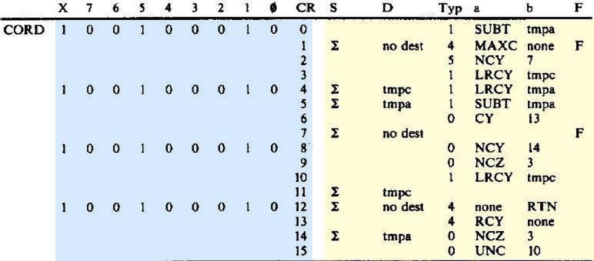
The 8086's microcode is much simpler than in most processors, but it's still fairly complex. The code below is the microcode routine from the 8086 for a routine called "CORD", part of integer division, consisting of 16 micro-instructions. I'm not going to explain how this microcode works in detail, but I want to give a flavor of it. Each line has an address on the left (blue) and the micro-instruction on the right (yellow), specifying the low-level actions during one time step (i.e. clock cycle). Each micro-instruction performs a move, transferring data from a source register (S) to a destination register (D). (The source Σ indicates the ALU output.) For parallelism, the micro-instruction performs an operation or two at the same time as the move. This operation is specified by the "a" and "b" fields; their meanings depend on the type field. For instance, type 1 indicates an ALU instruction such as subtract (SUBT) or left-rotate through carry (LRCY). Type 4 selects two general operations such as "RTN" which returns from a microcode subroutine. Type 0 indicates a jump operation; "UNC 10" is an unconditional jump to line 10 while "CY 13" jumps to line 13 if the carry flag is set. Finally, the "F" field indicates if the condition code flags should be updated. The key points are that the micro-instructions are simple and execute in one clock cycle, they can perform multiple operations in parallel to maximize performance, and they include control-flow operations such as conditional jumps and subroutines.

An example of a microcode routine. The CORD routine implements integer division with subtracts and left rotates. This is from patent 4,449,184.

An example of a microcode routine. The CORD routine implements integer division with subtracts and left rotates. This is from patent 4,449,184.

Each instruction is stored at a 13-bit address (blue) which consists of 9 bits shown explicitly and a 4-bit sequence counter "CR". The eight numbered address bits usually correspond to the machine instruction's opcode. The "X" bit is an extra bit to provide more address space for code that is not directly tied to a machine instruction, such as reset and interrupt code, address computation, and the multiply/divide algorithms.

A micro-instruction is encoded into 21 bits as shown below. Every micro-instruction contains a move from a source register to a destination register, each specified with 5 bits. The meaning of the remaining bits is a bit tricky since it depends on the type field, which is two or three bits long. The "short jump" (type 0) is a conditional jump within the current block of 16 micro-instructions. The ALU operation (type 1) sets up the arithmetic-logic unit to perform an operation. Bookkeeping operations (type 4) are anything from flushing the prefetch queue to ending the current instruction. A memory read or write is type 6. A "long jump" (type 5) is a conditional jump to any of 16 fixed microcode locations (specified in an external table). Finally, a "long call" (type 7) is a conditional subroutine call to one of 16 locations (different from the jump targets).

The encoding of a micro-instruction into 21 bits. Based on NEC v. Intel: Will Hardware Be Drawn into the Black Hole of Copyright?

The encoding of a micro-instruction into 21 bits. Based on NEC v. Intel: Will Hardware Be Drawn into the Black Hole of Copyright?

This "vertical" microcode format reduces the storage required for the microcode by encoding control signals into various fields. However, it requires some decoding logic to process the fields and generate the low-level control signals. Surprisingly, there's no specific "microcode decoder" circuit. Instead, the logic is scattered across the chip, looking for various microcode bit patterns to generate control signals where they are needed.

How instructions map onto the ROM

One interesting issue is how the micro-instructions are organized in the ROM, and how the right micro-instructions are executed for a particular machine instruction. The 8086 uses a clever mapping from the machine instruction to a microcode address that allows machine instructions to share microcode.

Different processors use a variety of approaches to microcode organization. One technique is for each micro-instruction to contain a field with the address of the next micro-instruction. This provides complete flexibility for the arrangement of micro-instructions, but requires a field to hold the address, increasing the number of bits in each micro-instruction. A common alternative is to execute micro-instructions sequentially, with a micro-program-counter stepping through each micro-address unless there is an explicit jump to a new address. This approach avoids the cost of an address field in each instruction, but requires a program counter with an incrementer, increasing the hardware complexity.

The 8086 uses a hybrid approach. A 4-bit program counter steps through the bottom 4 bits of the address, so up to 16 micro-instructions can be executed in sequence without a jump. This approach has the advantage of requiring a smaller 4-bit incrementer for the program counter, rather than a 13-bit incrementer. The microcode engine provides a "short jump" operation that makes it easy to jump within the group of 16 instructions using a 4-bit jump target, rather than a full 13-bit address.

Another important design decision in microcode is how to determine the starting micro-address for each machine instruction. In other words, if you want to do an ADD, where does the microcode for ADD start? One approach is a table of starting addresses: the system looks in the table to find the starting address for ADD, but this requires a large table of 256 entries. A second approach is to use the opcode code value as the starting address. That is, an ADD instruction 0x05 would start at micro-address 5. This approach has two problems. First, you can't run the microcode sequentially since consecutive micro-instructions belong to different machine instructions. Moreover, you can't share microcode since each instruction has a different address in the microcode ROM.

The 8086 solves these problems in two ways. First, the machine instructions are spaced sixteen slots apart in the microcode. In other words, the opcode is multiplied by 16 (has four zeros appended) to form the starting address in the microcode ROM, so there is plenty of space to implement each machine instruction. The second technique is that the ROM's addressing is partially decoded rather than fully decoded, so multiple micro-addresses can correspond to the same physical storage.4

To make this concrete, consider the 8086's arithmetic-logic instructions: one-byte add register to memory, one-byte add memory to register, one-word subtract memory from register, one-word xor register to memory, and so forth. There are 8 ALU operations and each can be byte- or word-sized, with memory as source or destination. This yields 32 different machine opcodes. These opcodes were carefully assigned, so they all have the format 00xxx0xx. The ROM address decoder is designed to look for three 0 bits in those positions, and ignore the other bits, so it will match that pattern. The result is that all 32 of these ALU instructions activate the same ROM column select line, and thus they all share the same microcode, shrinking the size of the ROM.

The microcode ROM's physical layout

The microcode ROM holds 512 words of 21 bits, so the obvious layout would be 512 columns and 21 rows. However, these dimensions are not practical for physically building the ROM because it would be too long and skinny. Instead, the ROM is constructed by grouping four words in each column, resulting in 128 columns of 84 rows, much closer to square. Not only does this make the physical layout more convenient, but it also reduces the number of column decoders from 512 to 128, reducing the circuitry size. Although the ROM now requires 21 multiplexers to select which of the four rows corresponds to each output bit, the circuitry is still much smaller. There is a tradeoff with the ability to merge addresses together by ignoring bits, though. Each decoder now selects a column of four words, rather than a single word, so each block of four words must have consecutive addresses.

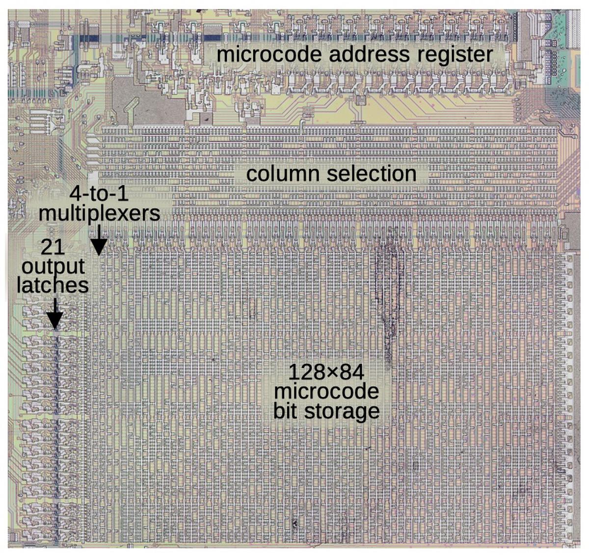
The main components of the microcode engine. The metal layer has been removed to show the silicon and polysilicon underneath. If you zoom in, the bit pattern is visible in the silicon doping pattern.

The main components of the microcode engine. The metal layer has been removed to show the silicon and polysilicon underneath. If you zoom in, the bit pattern is visible in the silicon doping pattern.

The image above shows how microcode is stored and accessed. At the top is the 13-bit microcode address register, which will be discussed in detail below. The column selection circuit decodes 11 of the 13 address bits to select one column of the microcode storage. At the left, multiplexers select one bit out of each four rows using the two remaining address bits (specifically, the two lowest sequence bits). The selected 21 microcode outputs are latched and fed to the rest of the processor, where they are decoded as described earlier and control the processor's actions.

Optimizing the microcode

In 1978, the number of bits that could be stored in the microcode ROM was rather limited. In particular, the 8086 holds only 512 micro-instructions. Since it has approximately 256 machine-code instructions in its one-byte opcode, combined with multiple addressing modes, and each instruction requires multiple micro-instructions, compression and optimization were necessary to make the microcode fit.5 The main idea was to move functionality out of the microcode and into discrete logic when it made sense. I'll describe some of the ways they did this.

The 8086 has an arithmetic-logic unit (ALU) that performs operations such as addition and subtraction, as well as logical operations such as AND and XOR. Consider the machine instruction ADD, implemented with a few micro-operations that compute the memory address, fetch data, perform the addition, and store the result. The machine instructions for subtraction, AND, or XOR require identical steps, except that the ALU performs a different operation. In total, the 8086 has eight ALU-based operations that are identical except for the operation performed by the ALU.6 The 8086 uses a "trick" where these eight machine instructions share the same microcode. Specifically, the microcode tells the ALU to perform a special operation XI, which indicates that the ALU should look at the appropriate bits of the instruction and do the appropriate operation.7 This shrinks the microcode for these operations by a factor of eight, at the cost of requiring additional logic for the ALU. In particular, the ALU control circuitry has a register to hold the relevant instruction bits, and a PLA to decode these bits into low-level ALU control signals.

Similarly, the 8086 has eight machine instructions to increment a specific register (out of a set of 8), and eight instructions to decrement a register. All 16 instructions are handled by the same set of micro-instructions and the ALU does the increment or decrement as appropriate. Moreover, the register control circuitry determines which register is specified by the instruction, without involvement from the microcode.

Another optimization is that the 8086 has many machine instructions in pairs: an 8-bit version and a 16-bit version. One approach would be to have separate microcode for the two instructions, one to handle a single byte and one to handle two bytes. Instead, the machine instructions share microcode. The complexity is moved to the circuitry that moves data on the bus: it looks at the low bit of the instruction to determine if it should process a byte or a word. This cuts the microcode size in half for the many affected instructions.

Finally, simple instructions that can take place in one cycle are implemented with logic gates, rather than through microcode. For instance, the CLC (clear carry flag) instruction updates the flag directly. Similarly, prefix instructions for segment selection, instruction locking, or repetition are performed in logic. These instructions don't use any microcode at all, which will be important later below.

Using techniques such as these, about 75 different instruction types are implemented in the microcode (instead of about 256), making the microcode much smaller. The tradeoff is that the 8086 requires more logic circuitry, but the designers found the tradeoff to be worthwhile.

The ModR/M byte

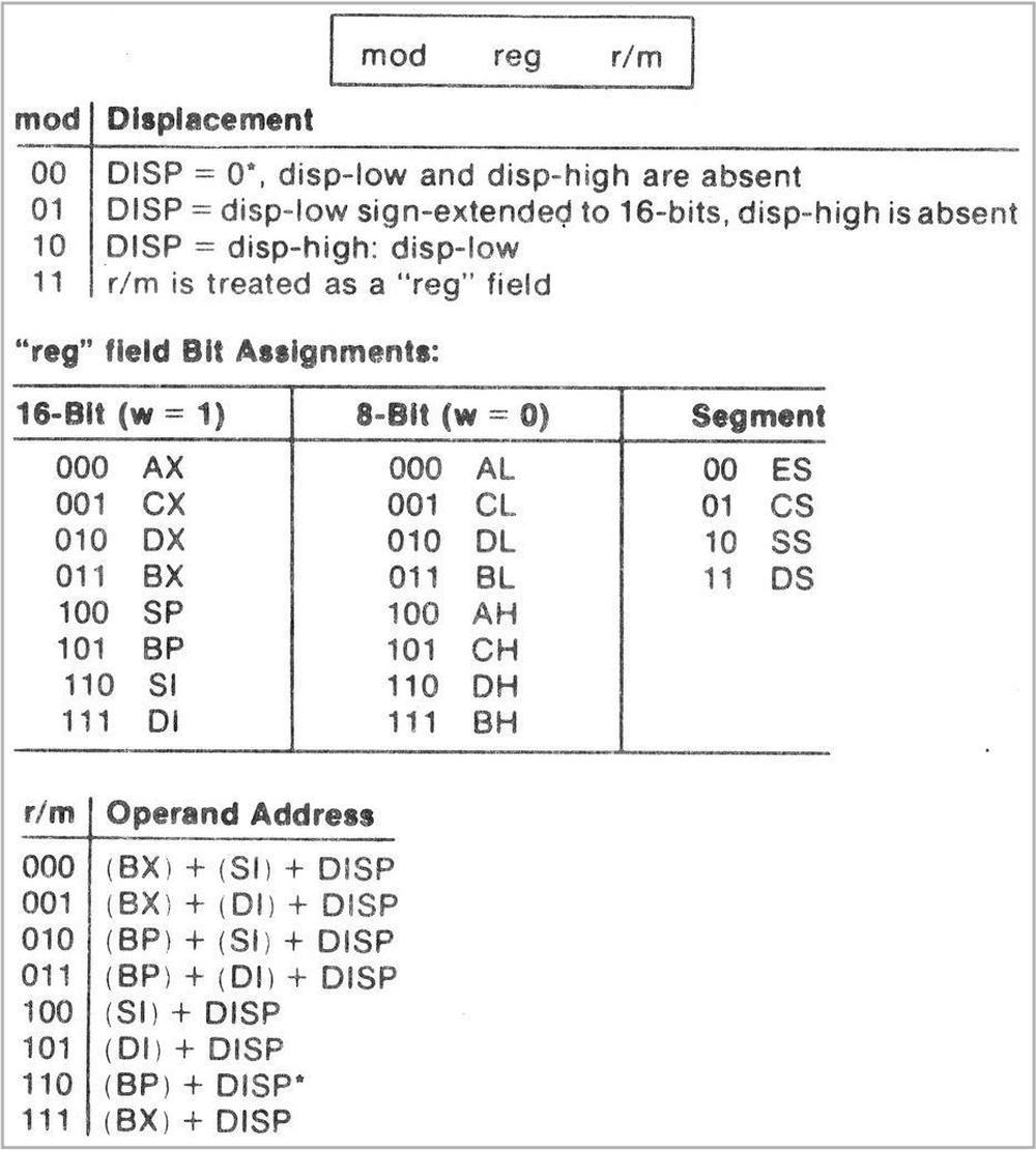
There's another complication for 8086 microcode, however. Most 8086 instructions have a second byte: the ModR/M byte, which controls the addressing mode for the instructions in a complex way (shown below). This byte gives 8086 instructions a lot of flexibility: you can use two registers, a register and a memory location, or a register and an "immediate" value specified in the instruction. The memory location can be specified by 8 index register combinations with a one-byte or two-byte displacement optionally added. (This is useful for accessing data in an array or structure, for instance.) Although these addressing modes are powerful, they pose a problem for the microcode.

A summary of the ModR/M byte, from MCS-86 Assembly Language Reference Guide.

A summary of the ModR/M byte, from MCS-86 Assembly Language Reference Guide.

These different addressing modes need to be implemented in microcode, since different addressing modes require different sequences of steps. In other words, you can't use the previous trick of pushing the problem into logic gates. And you clearly don't want a separate implementation of each instruction for each addressing mode since the size of the microcode would multiply out of control.

The solution is to use a subroutine (in microcode) to compute the memory address. Thus, instructions can share the microcode for each addressing mode. This adds a lot of complexity to the microcode engine, however, since it needs to store the micro-address for a micro-subroutine-call so it can return to the right location. To support this, the microcode engine has a register to hold this return address. (Since it doesn't have a full stack, you can't perform nested subroutine calls, but this isn't a significant limitation.)

The microcode ends up having about 10 subroutines for the different addressing modes, as well as four routines for the different sizes of displacement. (The 8 possibilities for source registers are handled in the register selection logic, rather than microcode.) Thus, the microcode handles the 256 different addressing modes with about 14 short routines that add the appropriate address register(s) and the displacement to obtain the memory address.

One more complication is that machine instructions can switch the source and destination specified by the ModR/M byte, depending on the opcode. For example, one subtract instruction will subtract a memory location from a register, while a different subtract instruction subtracts a register from a memory location. The two variants are distinguished by bit 1 of the instruction, the "direction" bit. These variants are handled by the control logic, so the microcode can ignore them. Specifically, before the source and destination specifications go to the register control circuitry, a crossover circuit can swap them based on the value of the direction bit.

The Translation ROM

As explained above, the starting address for a machine instruction is derived directly from the instruction's opcode. However, the microcode engine needs a mechanism to provide the address for jump and call operations. In the 8086, this address is hard-coded into the Translation ROM, which provides a 13-bit address.8 It holds ten destination addresses for jump operations and ten (different) addresses for call operations.

A second role of the Translation ROM is to hold target addresses for each ModR/M addressing mode, pointing to the code to compute the effective address. As a complication, two of the jump table entries in the Translation ROM are implemented with conditional logic, depending on whether or not the instruction's memory address calculation includes a displacement. By wiring this condition into the Translation ROM, the microcode avoids the need to test this condition.

The image below shows how the Translation ROM appears on the die. It is implemented as a partially-decoded ROM with multiplexed inputs.9 The inputs are at the bottom left. For a jump or call, the ROM uses 4 input bits from the microcode output, since the microcode selects the jump targets. For an address computation, it takes 5 bits from the instruction's ModR/M byte, so the routine is selected by the instruction. The ROM has additional input bits to select the mode (jump, call, or address) and for the conditional jumps. The decoding logic (left half) activates a row in the right half, generating the output address. This address exits at the bottom and is loaded into the micro-address register below the Translation ROM.

The Translation ROM holds addresses of routines in the microcode.

The Translation ROM holds addresses of routines in the microcode.

The Group Decode ROM

In the discussion above, I've discussed how various categories of instructions are optimized. For instance, many instructions have a bit that selects if they act on a byte or a word. Many instructions have a bit to reverse the direction of the operation's memory and register accesses. These features are implemented in logic rather than microcode. Other instructions are implemented outside microcode entirely. How does the 8086 determine which way to process an instruction?

The Group Decode ROM takes an instruction opcode and generate 15 signals that indicate various categories of instructions that are handled differently.10 The outputs from the Group Decode ROM are used by various logic circuits to determine how to handle the instruction. Some cases affect the microcode, for instance calling a microcode addressing routine if the instruction has a ModR/M byte. In other cases, these signals act "downstream" of the microcode, for example to determine if the operation should act on a byte or a word. Other signals cause the microcode to be bypassed completely.

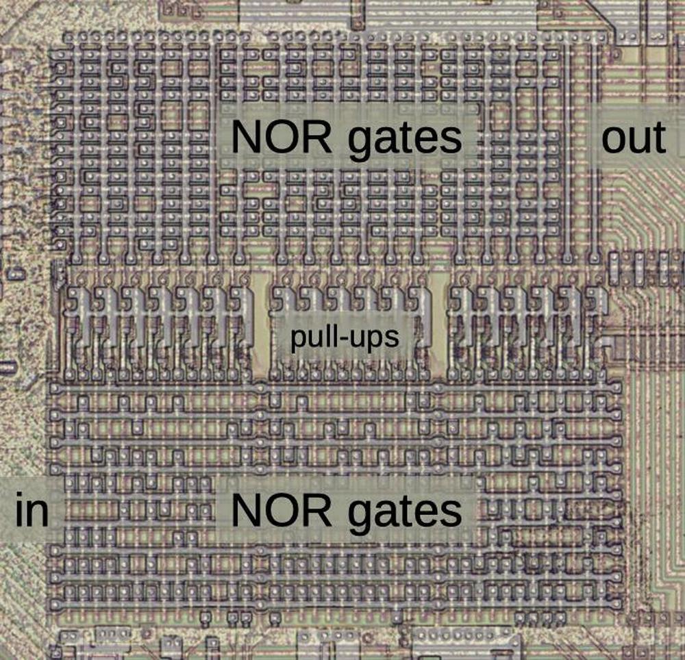
A closeup of the Group Decode ROM. The circuit uses two layers of NOR gates to generate the output signals from the opcode inputs. This image shows a composite of the metal, polysilicon, and silicon layers.

A closeup of the Group Decode ROM. The circuit uses two layers of NOR gates to generate the output signals from the opcode inputs. This image shows a composite of the metal, polysilicon, and silicon layers.

Specially-encoded instructions

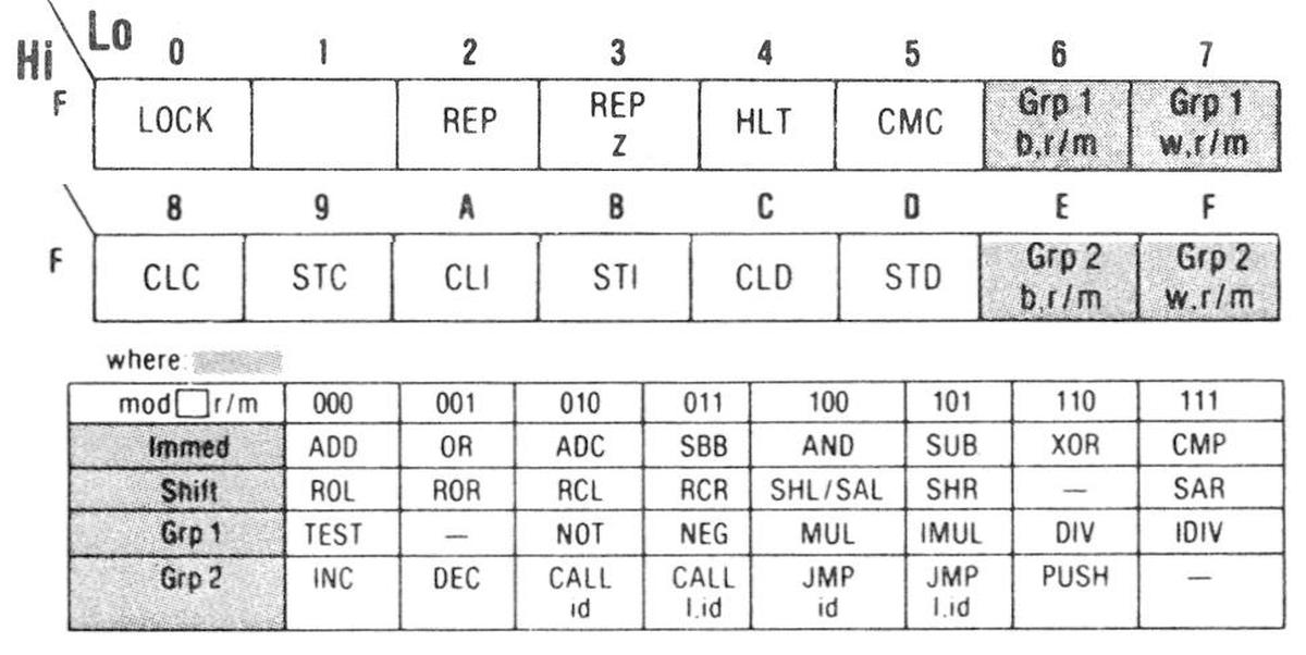
For most of the 8086 instructions, the first byte specifies the instruction. However, the 8086 has a few instructions where the ModR/M byte completely changes the meaning of the first byte. For instance, opcode 0xF6 (Grp 1 below) can be a TEST, NOT, NEG, MUL, IMUL, DIV, or IDIV instruction based on the value of the ModR/M byte. Similarly, opcode 0xFE (Grp 2) indicates an INC, DEC, CALL, JMP, or PUSH instruction.11

The 8086 instruction map for opcodes 0xF0 to 0xFF. Based on MCS-86 Assembly Language Reference Guide.

The 8086 instruction map for opcodes 0xF0 to 0xFF. Based on MCS-86 Assembly Language Reference Guide.

This encoding may seem a bit random, but there's a reason behind it. Most instructions act on a source and a destination. But some, such as INC (increment) use the same register or memory location for the source and the destination. Others, such as CALL or JMP, only use one address. Thus, the "reg" field in the ModR/M byte is redundant. Since these bits would be otherwise "wasted", they are used instead to specify different instructions. (There are only 256 single-byte opcodes, so you want to make the best use of them.)

The implementation of these instructions in microcode is interesting. Since the instructions share the same first byte, the standard microcode mapping would put them at the same microcode address. However, these instructions are treated specially, with the "reg" field from the ModR/M byte copied into the lower bits of the microcode address. In effect, the instructions are treated as opcodes 0xF0 through 0xFF, so the different instruction variants execute at separate microcode addresses. You might expect a collision with the opcodes that really have the values 0xF0 through 0xFF. However, the 8086 opcodes were cleverly arranged so none of the other instructions in this range use microcode. As you can see above, the other instructions are prefixes (LOCK, REP, REPZ), halt (HLT), or flag operations (CMC, CLC, STC, CLI, STI, CLD, STD), all implemented outside microcode. Thus, the range 0xF0-0xFF is freed up for the "expanded" instructions.

The hardware implementation for this is not too complex. The Group ROM produces an output for these special instructions. This causes the microcode address register to load the appropriate bits from the ModR/M byte, causing the appropriate microcode routine to be executed.

The microcode address register

The heart of the microcode engine is the microcode address register, which determines which microcode address to execute. As described earlier, the microcode address is 13 bits, of which 8 bits generally correspond to the instruction opcode, one bit is an extra "X" instruction bit, and 4 bits are sequentially incremented. The diagram below shows how the circuitry for the bits is arranged. The 9 instruction bits each have a nearly-identical circuit. The sequence bits have more circuitry and each one is different, because the circuit to increment the address is different for each bit.

Layout of the microcode address register. Each bit has a roughly vertical block of circuitry.

Layout of the microcode address register. Each bit has a roughly vertical block of circuitry.

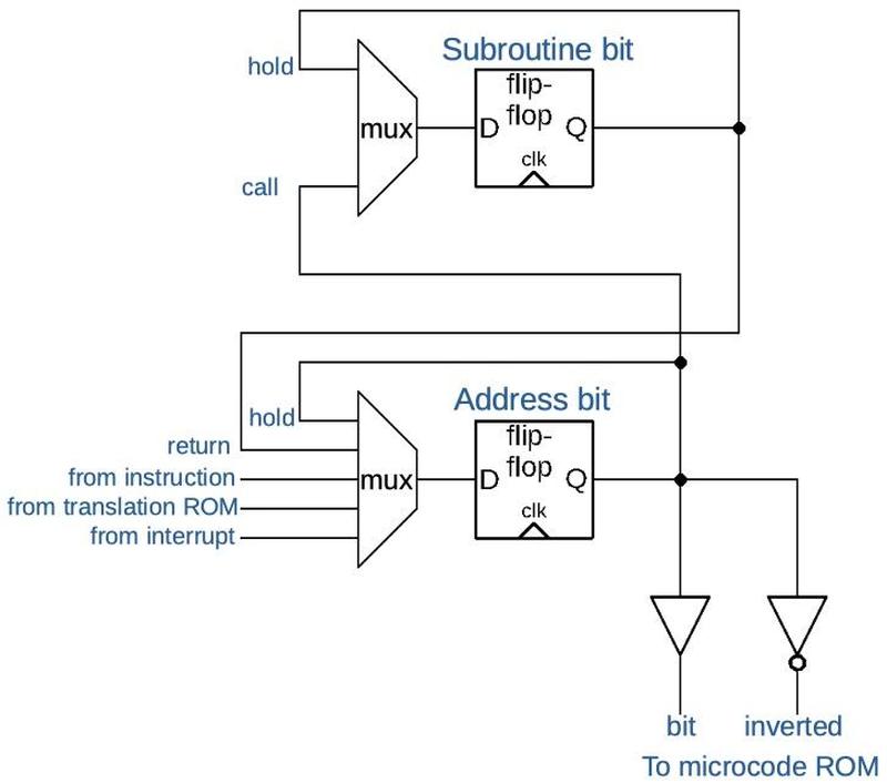
The schematic below shows the circuitry for one bit in the microcode address register. It has two flip-flops: one to hold the current address bit and one to hold the old address while performing a subroutine call. A multiplexer (mux) selects the input to each flip-flop. For instance, if the microcode is waiting for a memory access, the "hold" input to the multiplexer causes the current address to loop around and get reloaded into the flip-flop. For a subroutine call, the "call" input saves the current address in the subroutine flip-flop. Conversely, when returning from a subroutine, the "return" input loads the old address from the subroutine flip-flop. The address flip-flop also has inputs to load the instruction as the address, to load an address from the translation ROM, or to load an interrupt microcode handler address. The circuit sends the address bit (and inverted address bit) to the microcode ROM's address decoder.

Schematic of a typical bit in the microcode address register.

Schematic of a typical bit in the microcode address register.

Each bit has some special-case handling, so this schematic should be viewed as an illustration, not an accurate wiring diagram. In particular, the sequence bits also have inputs from the incrementer, so they can step to the next address. The low-order bits have instruction inputs to handle the specially-encoded "group" instructions discussed in the previous section.

The control signals for the multiplexers are generated from various sources. A circuit called the loader starts processing of an instruction, synchronized to the prefetch queue and instruction fetch from memory. The call and return operations are microcode instructions. The Group Decode ROM controls some of the inputs, for instance to process a ModR/M byte. Thus, there is a moderate amount of conditional logic that determines the microcode address and thus what microcode gets executed.

Conclusions

This has been a lot of material, so thank you for sticking with it to the end. I draw three conclusions from studying the microcode engine of the 8086. First, the implementation of microcode is considerably more complex than the clean description of microcode that is presented in books. A lot of functionality is implemented in logic outside of microcode, so it's not a "pure" microcode implementation. Moreover, there are many optimizations and corner cases. The microcode engine has two supporting ROMs: the Translation ROM and the Group Decode ROM. Even the microcode address register has complications.

Second, the need for all these optimizations shows how the 8086 was just on the edge of what was practical. The designers clearly went to a lot of effort to get the microcode to fit in the space available.

Finally, looking at the 8086 in detail shows how complex its instruction set is. I knew in the abstract that it was much more convoluted than, say, an ARM chip. But seeing all the special case circuitry on the die to handle the corner cases of the instruction set really makes this clear.

I plan to continue reverse-engineering the 8086 die so follow me on Twitter @kenshirriff or RSS for updates. I've also started experimenting with Mastodon recently as @[email protected]. If you're interested in the 8086, I wrote about the 8086 die, its die shrink process and the 8086 registers earlier.

Notes and references

  1. The 8086 microcode was disassembled (link) a couple of years ago by Andrew Jenner by extracting the bits from my die photos. My post here is a bit different, looking at hardware that runs the microcode, rather than the contents of the microcode. 

  2. According to Wikipedia, the Zilog Z8000 (1979) didn't use microcode, which is a bit surprising for that timeframe. This design decision had the advantage of reducing transistor count, but the disadvantage of hard-to-fix logic bugs in the instruction decoder. 

  3. As an example of a non-microcoded processor, the MOS 6502 (1975) used a PLA (Programmable Logic Array) to perform much of the decoding (details). A PLA provides a structured way of implementing logic gates in a relatively dense array. A PLA is kind of like a ROM—a PLA can implement a ROM and vice versa—so it can be hard to see the difference. The usual distinction is that only one row of a ROM is active at a time, the address that you're reading out. A PLA is more general since multiple rows can be active at a time, combined to form the outputs.

    The Z80 had a slightly different implementation. It used a smaller PLA to perform basic decoding of instructions into various types. It then generated control signals through a large amount of "random" logic (so-called because of its appearance, not because it's actually random). This logic combined instruction types and timing signals to generate the appropriate control signals. 

  4. In a "normal" ROM, the address bits are decoded with logic gates so each unique address selects a different storage column in the ROM. However, parts of the decoder circuitry can "ignore" bits so multiple addresses select the same storage column. For a hypothetical example, suppose you're decoding 5-bit addresses. Instead of decoding 11010 and 11011 separately, you could ignore the last bit so both addresses access the same ROM data. or you could ignore the last three bits so all 8 addresses of the form 11xxx go to the same ROM location (where x indicates a bit that can be either 0 or 1). This makes the ROM more like a PLA (Programmable Logic Array), but still accessing a single row at a time. 

  5. The Intel 8087 was the floating point co-processor for the 8086. The 8087 required a lot of microcode, more than could fit in a standard ROM on the die. To get the microcode to fit, Intel created a special ROM that stored two bits per transistor (instead of one) by using four different sizes of transistors to generate four different voltages. Analog circuitry converted each voltage level into two bits. This complex technique doubled the density (at least in theory), allowing the microcode to fit on the chip. I wrote about the 8087's non-binary ROM here

  6. The ALU operations that are grouped together are add, add with carry, subtract, subtract with borrow, logical AND, logical XOR, logical OR, and compare. The compare operation may seem out of place in this list, but it is implemented as a subtract operation that updates the condition flags without changing the value. Operations such as increment, decrement, negation, and logical NOT may seem like they should be included, but since they operate on a single argument instead of two, they are implemented differently at the microcode level. Increment and decrement are combined in the microcode, however. Negation and logical NOT could be combined except that negation affects the condition code flags, while NOT doesn't, so they need separate microcode. (This illustrates how subtle features of the instruction set can have more impact than you might expect.) Since the ALU doesn't have hardware multiplication and division, the multiplication and division operations are implemented separately in microcode with loops. 

  7. The ALU itself isn't examining instruction bits to decide what to do. There's some control circuitry next to the ALU that uses a PLA (Programmable Logic Array) to examine the instruction bits and the microcode's ALU command to generate low-level control signals for the ALU. These signals control things such as carry propagation, argument negation, and logical operation selection to cause the ALU to perform the desired operation. 

  8. The Translation ROM has one additional output: a wire indicating an address mode that uses the BP register. This output goes to the segment register selection circuitry and selects a different segment register. The reason is that the 8086 uses the Data Segment by default for effective address computation, unless the address mode uses BP as a base register. In that case, the Stack Segment is used. This is an example of how the 8086 architecture is not orthogonal and has lots of corner cases. 

  9. You can also view the Translation ROM as a PLA (Programmable Logic Array) constructed from two layers of NOR gates. The conditional entries make it seem more like a PLA than a ROM. Technically, it can be considered a ROM since a single row is active at a time. I'm using the name "Translation ROM" because that's what Intel calls it in the patents. 

  10. Although the Group Decode ROM is called a ROM in the patent, I'd consider it more of a PLA (programmable logic array). Conceptually it holds 256 words, one for each instruction. But its implementation is an array of logic functions. 

  11. These instructions were called "Group 1" and "Group 2" instructions in the 8086 documentation. Later Intel documentation renamed them as "Unary Group 3", "INC/DEC Group 4" and "Indirect Group 5". Some details are here. The 8086 has two other groups of instructions where the reg field defines the instruction: the "Immediate" instructions 0x80-0x83 and the "Shift" instructions 0xD0-0xD3. For these opcodes, the different instructions were implemented by the ALU. As far as the microcode was concerned, these were "normal" instructions so I won't discuss them in this post.

    I should mention that although the 8086 opcodes are always expressed in hexadecimal, the encoding makes much more sense if you look at it in octal. Details here. The octal encoding also applies to other related chips including the 8008, 8080, and Z80. 

A bug fix in the 8086 microprocessor, revealed in the die's silicon

The 8086 microprocessor was a groundbreaking processor introduced by Intel in 1978. It led to the x86 architecture that still dominates desktop and server computing. While reverse-engineering the 8086 from die photos, a particular circuit caught my eye because its physical layout on the die didn't match the surrounding circuitry. This circuit turns out to implement special functionality for a couple of instructions, subtlely changing the way they interacted with interrupts. Some web searching revealed that this behavior was changed by Intel in 1978 to fix a problem with early versions of the 8086 chip. By studying the die, we can get an idea of how Intel dealt with bugs in the 8086 microprocessor.

In modern CPUs, bugs can often be fixed through a microcode patch that updates the CPU during boot.1 However, prior to the Pentium Pro (1995), microprocessors could only be fixed through a change to the design that fixed the silicon. This became a big problem for Intel with the famous Pentium floating-point division bug. The chip turned out to have a bug that resulted in rare but serious errors when dividing. Intel recalled the defective processors in 1994 and replaced them, at a cost of $475 million.

The circuit on the die

The microscope photo below shows the 8086 die with the main functional blocks labeled. This photo shows the metal layer on top of the silicon. While modern chips can have more than a dozen layers of metal, the 8086 has a single layer. Even so, the metal mostly obscures the underlying silicon. Around the outside of the die, you can see the bond wires that connect pads on the chip to the 40 external pins.

The 8086 die with main functional blocks labeled. Click this image (or any other) for a larger version.

The 8086 die with main functional blocks labeled. Click this image (or any other) for a larger version.

The relevant part of the chip is the Group Decode ROM in the upper center. The purpose of this circuit is to categorize instructions into groups that control how they are decoded and processed. For instance, very simple instructions (such as setting a flag) can be performed directly in one cycle. Other instructions are not complete instructions, but a prefix that modifies the following instruction. The remainder of the instructions are implemented in microcode, which is stored in the lower-right corner of the chip. Many of these instructions have a second byte, the "Mod R/M" byte that specifies a register and the memory addressing scheme. Some instructions have two versions: one for an 8-bit operand and one for a 16-bit operand. Some operations have a bit to swap the source and destination. The Group Decode ROM is responsible for looking at the 8 bits of the instruction and deciding which groups the instruction falls into.

A closeup of the Group Decode ROM. This image is a composite showing the metal, polysilicon, and silicon layers.

A closeup of the Group Decode ROM. This image is a composite showing the metal, polysilicon, and silicon layers.

The photo above shows the Group Decode ROM in more detail. Strictly speaking, the Group Decode ROM is more of a PLA (Programmable Logic Array) than a ROM, but Intel calls it a ROM. It is a regular grid of logic, allowing gates to be packed together densely. The lower half consists of NOR gates that match various instruction patterns. The instruction bits are fed horizontally from the left, and each NOR gate is arranged vertically. The outputs from these NOR gates feed into a set of horizontal NOR gates in the upper half, combining signals from the lower half to produce the group outputs. These NOR gates have vertical inputs and horizontal outputs.

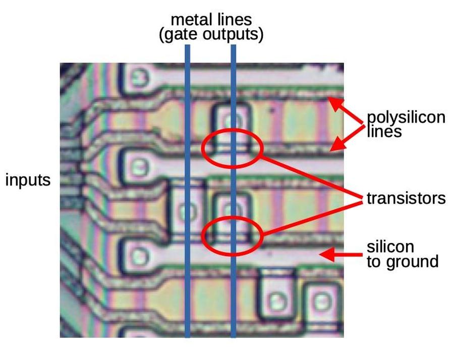
The diagram below is a closeup of the Group Decode ROM, showing how the NOR gates are constructed. The pinkish regions are silicon, doped with impurities to make it a semiconductor. The gray horizontal lines are polysilicon, a special type of silicon on top. Where a polysilicon crosses conductive silicon, it forms a transistor. The transistors are wired together by metal wiring on top. (I dissolved the metal layer with acid to show the silicon; the blue lines show where two of the metal wires were.) When an input is high, it turns on the corresponding transistors, pulling the vertical lines low. This creates NOR gates with multiple inputs. The key idea of the PLA is that at each point where horizontal and vertical lines cross, a transistor can be present or absent, to select the desired gate inputs. By doping the silicon in the desired pattern, transistors can be created or omitted as needed. In the diagram below, two of the transistors are highlighted. You can see that some of the other locations have transistors, while others do not. Thus, the PLA provides a dense, flexible way to produce a set of outputs from a set of inputs.

Cioseup of part of the Gate Decode ROM showing a few of the transistors. I dissolved the metal layer for this image, to reveal the silicon and polysilicon underneath.

Cioseup of part of the Gate Decode ROM showing a few of the transistors. I dissolved the metal layer for this image, to reveal the silicon and polysilicon underneath.

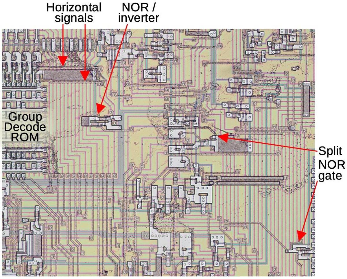
Zooming out a bit, the PLA is connected to some unusual circuitry, shown below. The last two columns in the PLA are a bit peculiar. The upper half is unused. Instead, two signals leave the side of the PLA horizontally and bypass the top of the PLA. These signals go to a NOR gate and an inverter that are kind of in the middle of nowhere, separated from the rest of the logic. The output from these gates goes to a three-input NOR gate, which is curiously split into two pieces. The lower part is a normal two-input NOR gate, but then the transistor for the third input (the one we're looking at) is some distance away. It's unusual for a gate to be split across a distance like this.

The circuitry as it appears on the die.

The circuitry as it appears on the die.

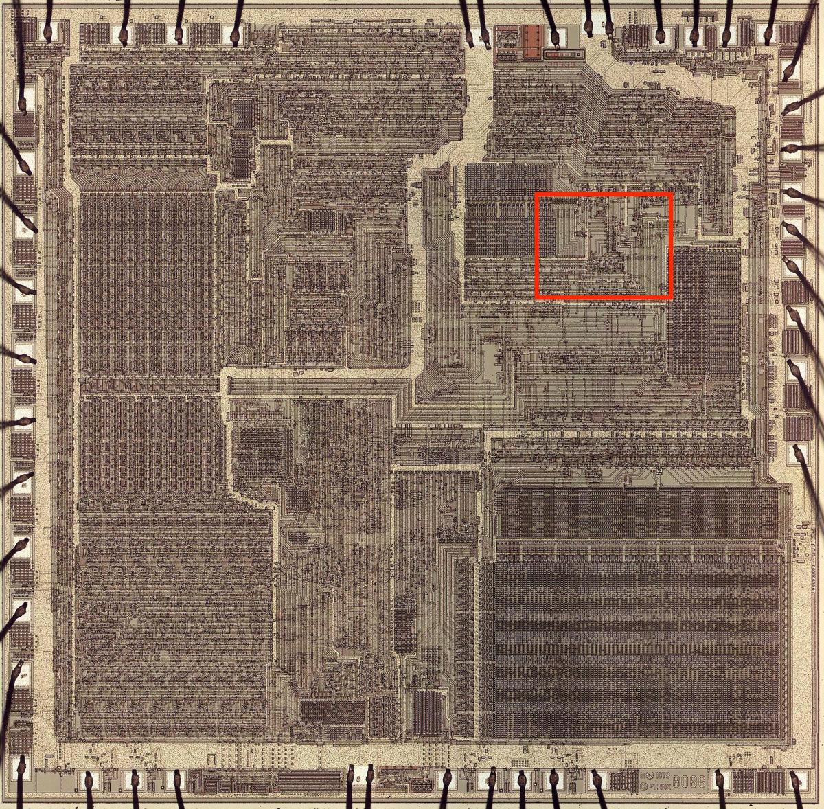
It can be hard to keep track of the scale of these diagrams. The highlighted box in the image below corresponds to the region above. As you can see, the circuit under discussion spans a fairly large fraction of the die.

The red rectangle in this figure highlights the region in the diagram above.

The red rectangle in this figure highlights the region in the diagram above.

My next question was what instructions were affected by this mystery circuitry. By looking at the transistor pattern in the Group Decode ROM, I determined that the two curious columns matched instructions with bits 10001110 and 000xx111. A look at the 8086 reference shows that the first bit pattern corresponds to the instructions MOV sr,xxx, which loads a value into a segment register. The second bit pattern corresponds to the instructions POP sr, which pops a value from the stack into a segment register. But why did these instructions need special handling?

The interrupt bug

After searching for information on these instructions, I came across errata stating: "Interrupts Following MOV SS,xxx and POP SS Instructions May Corrupt Memory. On early Intel 8088 processors (marked “INTEL ‘78” or “(C) 1978”), if an interrupt occurs immediately after a MOV SS,xxx or POP SS instruction, data may be pushed using an incorrect stack address, resulting in memory corruption." The fix to this bug turns out to be the mystery circuitry.

I'll give a bit of background. The 8086, like most processors, has an interrupt feature where an external signal, such as a timer or input/output, can interrupt the current program. The processor starts running different code to handle the interrupt, and then returns to the original program, continuing where it left off. When interrupted, the processor uses its stack in memory to keep track of what it was doing in the original program so it can continue. The stack pointer (SP) is a register that keeps track of where the stack is in memory.

A complication is that the 8086 uses "segmented memory", where memory is divided into chunks (segments) with different purposes. On the 8086, there are four segments: the Code Segment, Data Segment, Stack Segment, and Extra Segment. Each segment has an associated segment register that holds the starting memory address for that segment. Suppose you want to change the location of the stack in memory, maybe because you're starting a new program. You need to change the Stack Segment register (called SS) to point to the new location for the stack segment. And you also need to change the Stack Pointer register (SP) to point to the stack's current position within the stack segment.

A problem arises if the processor receives an interrupt after the Stack Segment register has been changed, but before the Stack Pointer register has been changed. The processor will store information on the stack using the old stack pointer address but in the new segment. Thus, the information is stored into essentially a random location in memory, which is bad.2 Intel's fix was to delay an interrupt after an update to the stack segment register, so you had a chance to update the stack pointer.3 The stack segment register could be changed in two ways. First, you could move a value to the register ("MOV SS, xxx" in assembly language), or you could pop a value off the stack into the stack segment register ("POP SS"). These are the two instructions affected by the mystery circuitry. Thus, we can see that Intel added circuitry to delay an interrupt immediately after one of these instructions and avoid the bug.

Conclusions

One of the interesting things about reverse-engineering the 8086 is when I find a curious feature on the die and then find that it matches an obscure part of the 8086 documentation. Most of these are deliberate design decisions, but they show how complex and ad-hoc the 8086 architecture is, with many special cases. Each of these cases results in some circuitry and gates, complicating the chip. (In comparison, I've reverse-engineered the ARM1 processor, a RISC processor that started the ARM architecture. The ARM1 has a much simpler architecture with very few corner cases. This is reflected in circuitry that is much simpler.)

The case of the segment registers and interrupts, however, is the first circuit that I've found on the 8086 die that is part of a bug fix. This fix appears to have been fairly tricky, with multiple gates scattered in unused parts of the chip. It would be interesting to get a die photo of a very early 8086 chip, prior to this bug fix, to confirm the change and see if anything else was modified.

If you're interested in the 8086, I wrote about the 8086 die, its die shrink process and the 8086 registers earlier. I plan to write more about the 8086 so follow me on Twitter @kenshirriff or RSS for updates. I've also started experimenting with Mastodon recently as @[email protected].

Notes and references

  1. The modern microcode update process is more complicated than I expected with updates possible before the BIOS is involved, during boot, or even while applications are running. Intel provides details here. Apparently Intel originally added patchable microcode to the Pentium Pro for chip debugging and testing, but realized that it would be a useful feature to fix bugs in the field (details). 

  2. The obvious workaround for this problem is to disable interrupts while you're changing the Stack Segment register, and then turn interrupts back on when you're done. This is the standard way to prevent interrupts from happening at a "bad time". The problem is that the 8086 (like most microprocessors) has a non-maskable interrupt (NMI), an interrupt for very important things that can't be disabled. 

  3. Intel documents the behavior in a footnote on page 2-24 of the User's Manual:

    There are a few cases in which an interrupt request is not recognized until after the following instruction. Repeat, LOCK and segment override prefixes are considered "part of" the instructions they prefix; no interrupt is recognized between execution of a prefix and an instruction. A MOV (move) to segment register instruction and a POP segment register instruction are treated similarly: no interrupt is recognized until after the following instruction. This mechanism protects a program that is changing to a new stack (by updating SS and SP). If an interrupt were recognized after SS had been changed, but before SP had been altered, the processor would push the flags, CS and IP into the wrong area of memory. It follows from this that whenever a segment register and another value must be updated together, the segment register should be changed first, followed immediately by the instruction that changes the other value. There are also two cases, WAIT and repeated string instructions, where an interrupt request is recognized in the middle of an instruction. In these cases, interrupts are accepted after any completed primitive operation or wait test cycle.

    Curiously, the fix on the chip is unnecessarily broad: a MOV or POP for any segment register delays interrupts. There was no hardware reason for this: the structure of the PLA means that all the necessary instruction bits were present and it would be no harder to test for the Stack Segment register specifically. The fix of delaying interrupts after a POP or MOV remains in the x86 architecture today. However, it has been cleaned up so only instructions affecting the Stack Segment register cause the delay; operations on other segment registers have no effect. 

The unusual bootstrap drivers inside the 8086 microprocessor chip

The 8086 microprocessor is one of the most important chips ever created; it started the x86 architecture that still dominates desktop and server computing today. I've been reverse-engineering its circuitry by studying its silicon die. One of the most unusual circuits I found is a "bootstrap driver", a way to boost internal signals to improve performance.1

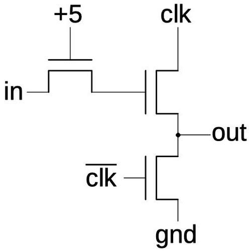
The bootstrap driver circuit from the 8086 processor.

The bootstrap driver circuit from the 8086 processor.

This circuit consists of just three NMOS transistors, amplifying an input signal to produce an output signal, but it doesn't resemble typical NMOS logic circuits and puzzled me for a long time. Eventually, I stumbled across an explanation:2 the "bootstrap driver" uses the transistor's capacitance to boost its voltage. It produces control pulses with higher current and higher voltage than otherwise possible, increasing performance. In this blog post, I'll attempt to explain how the tricky bootstrap driver circuit works.

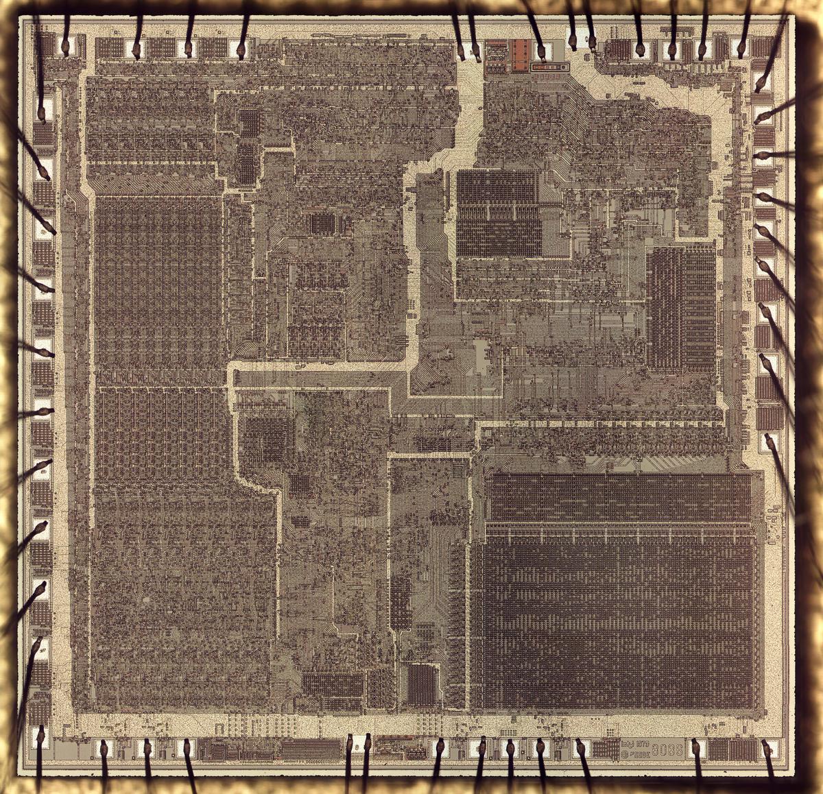
A die photo of the 8086 processor. The metal layer on top of the silicon is visible. Around the edge of the chip, bond wires provide connections to the chip's external pins. Click this image (or any other) for a larger version.

A die photo of the 8086 processor. The metal layer on top of the silicon is visible. Around the edge of the chip, bond wires provide connections to the chip's external pins. Click this image (or any other) for a larger version.

NMOS transistors

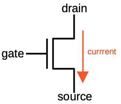
The 8086 is built from MOS transistors (MOSFETs), specifically NMOS transistors. Understanding the bootstrap driver requires some understanding of these transistors. If you're familiar with MOSFETs as components, they have source and drain pins and current flows from the drain to the source, controlled by the gate pin. Most of the time I treat an NMOS transistor as a digital switch between the drain and the source: a 1 input turns the transistor on, closing the switch, while a 0 turns the transistor off. However, for the bootstrap driver, we must consider the MOSFET in a bit more detail.

A MOSFET switches current from the drain to the source, under control of the gate.

A MOSFET switches current from the drain to the source, under control of the gate.

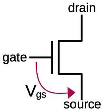
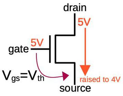
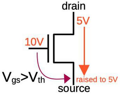
The important aspect of the gate is the difference between the gate voltage and the (typically lower) source voltage; this is denoted as Vgs. Without going into semiconductor physics, a slightly more accurate model is that the transistor turns on when the voltage between the gate and the source exceeds the fixed threshold voltage, Vth. This creates a conducting channel between the transistor's source and drain. Thus, if Vgs > Vth, the transistor turns on and current flows. Otherwise, the transistor turns off and no current flows.

The voltage between the gate and the source (Vgs) controls the transistor.

The voltage between the gate and the source (Vgs) controls the transistor.

The threshold voltage has an important consequence for a chip such as the 8086. The 8086, like most chips of that era, used a 5-volt power supply. The threshold voltage depends on manufacturing characteristics, but I'll use 1 volt as a typical value.3 The result is that if you put 5 volts on the drain and on the gate, the transistor can pull the source up to about 4 volts, but then Vgs falls to the threshold voltage and the transistor stops conducting. Thus, the transistor can't pull the source all the way up to the 5-volt supply, but falls short by a volt on the output. In some circumstances this is a problem, and this is the problem that the bootstrap driver fixes.

Due to the threshold voltage, the transistor doesn't pull the source all the way to the drain's voltage, but "loses" a volt.

Due to the threshold voltage, the transistor doesn't pull the source all the way to the drain's voltage, but "loses" a volt.

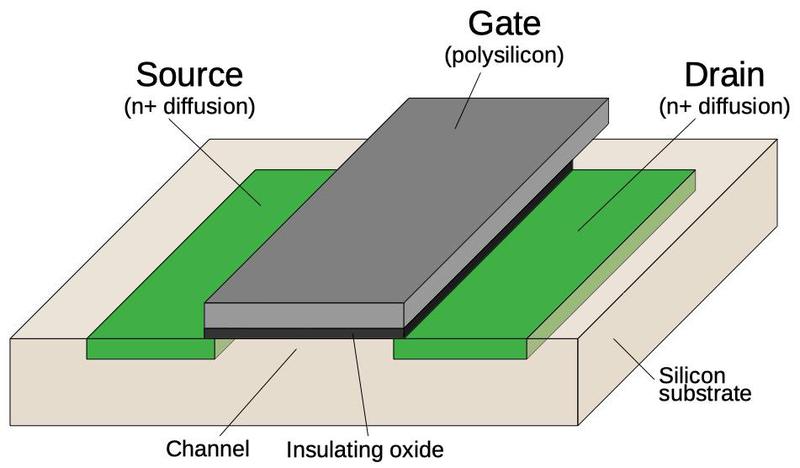
If you get a transistor as a physical component, the source and drain are not interchangeable. However, in an integrated circuit, there is no difference between the source and the drain, and this will be important.4 The diagram below shows how a MOSFET is constructed on the silicon die. The source and drain consist of regions of silicon doped with impurities to change their property. Between them is a channel of undoped silicon, which normally does not conduct. Above the channel is the gate, made of a special type of silicon called polysilicon. The voltage on the gate controls the conductivity of the channel. A very thin insulating layer separates the gate from the channel. As a side effect, the insulating layer creates some capacitance between the gate and the underlying silicon.

Diagram of an NMOS transistor in an integrated circuit.

Diagram of an NMOS transistor in an integrated circuit.

Basic NMOS circuits

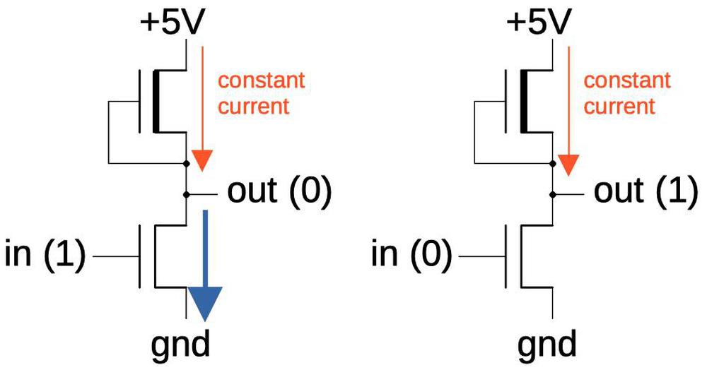
Before getting to the bootstrap driver, I'll explain how a basic inverter is implemented in an NMOS chip like the 8086. The inverter is built from two transistors: a normal transistor on the bottom, and a special load transistor on top that acts like a pull-up resistor, providing a small constant current.5 With a 1 input, the lower transistor turns on, pulling the output to ground to produce a 0 output. With a 0 input, the lower transistor turns off and the current from the upper transistor drives the output high to produce a 1 output. Thus, the circuit implements an inverter: producing a 1 when the input is 0 and vice versa.

A standard NMOS inverter is built from two transistors. The upper transistor is a "depletion load" transistor.

A standard NMOS inverter is built from two transistors. The upper transistor is a "depletion load" transistor.

The disadvantage of this inverter circuit is that when it produces a 0 output, current continuously flows through the load transistor and the lower transistor to ground. This wastes power, leading to high power consumption for NMOS circuitry. (To solve this, CMOS circuitry took over in the 1980s and is used in modern microprocessors.) This also limits the current that the inverter can provide.

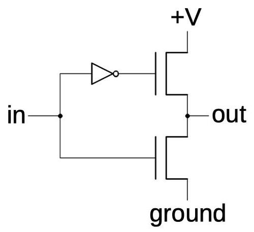
If a gate needs to provide a relatively large current, for instance to drive a long bus inside the chip, a more complex circuit is used, the "superbuffer". The superbuffer uses one transistor to pull the output high and a second transistor to pull the output low.6 Because only one transistor is on at a time, a high-current output can be produced without wasting power. There are two disadvantages of the superbuffer, though. First, the superbuffer requires an inverter to control the high-side transistor, so it uses considerably more space on the die. Second, the superbuffer can't pull the high output all the way up; it loses a volt due to the threshold voltage as described earlier.

Combining two output transistors with an inverter produces a higher-current output, known as a superbuffer.

Combining two output transistors with an inverter produces a higher-current output, known as a superbuffer.

The bootstrap driver

In some circumstances, you want both a high-current output, and the full output voltage. One example is connecting a register to an internal bus. Since the 8086 is a 16-bit chip, it uses 16 transistors for the bus connection. Driving 16 transistors in parallel requires a fairly high current. But the bus transistors are "pass" transistors, which lose a volt due to the threshold voltage, so you want to start with the full voltage, not already down one volt. To provide both high current and the full voltage, bootstrap drivers are used to control the buses, as well as similar tasks such as ALU control.

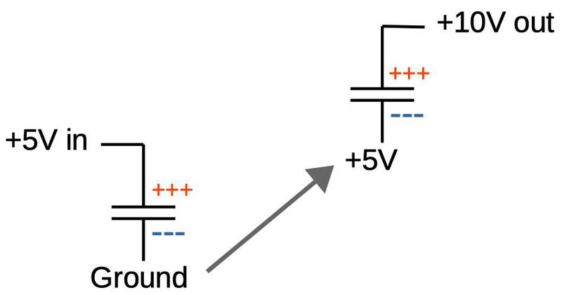
The concept behind the bootstrap driver is to drive the gate voltage significantly higher than 5 volts, so even after losing the threshold voltage, the transistor can produce the full 5-volt output.7 The higher voltage is generated by a charge pump, as illustrated below. Suppose you charge a capacitor with 5 volts. Now, disconnect the bottom of the capacitor from ground, and connect it to +5 volts. The capacitor is still charged with 5 volts, so now the high side is at +10 volts with respect to ground. Thus, a capacitor can be used to create a higher voltage by "pumping" the charge to a higher level.

On the left, the "flying capacitor' is charged to 5 volts. By switching the lower terminal to +5 volts, the capacitor now outputs +10 volts

On the left, the "flying capacitor' is charged to 5 volts. By switching the lower terminal to +5 volts, the capacitor now outputs +10 volts

The idea of the bootstrap driver is to attach a capacitor to the gate and charge it to 5 volts. Then, the low side of the capacitor is raised to 5 volts, boosting the gate side of the capacitor to 10 volts. With this high voltage on the gate, the threshold voltage is easily exceeded and the transistor can pass the full 5 volts from the drain to the source, producing a 5-volt output.

With a large voltage on the gate, the threshold voltage is exceeded and the transistor remains on until the source reaches 5 volts.

With a large voltage on the gate, the threshold voltage is exceeded and the transistor remains on until the source reaches 5 volts.

In the 8086 bootstrap driver,8 an explicit capacitor is not used.9 Instead, the transistor's inherent capacitance is sufficient. Due to the thin insulating oxide layer between the gate and the underlying silicon, the gate acts as the plate of a capacitor relative to the source and drain. This "parasitic" capacitance is usually a bad thing, but the bootstrap driver takes advantage of it.

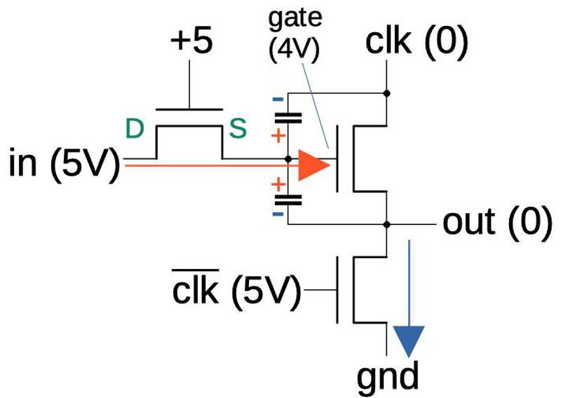
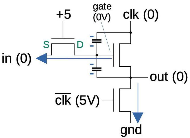
The diagrams below show how the bootstrap driver works. Unlike an inverter, the bootstrap driver is controlled by the chip's clock, generating an output only when the clock is high. In the first diagram, we assume that the input is a 1 and the clock is low (0). Two things happen. First, the inverted clock turns on the bottom transistor, pulling the output to ground. Second, the 5V input passes through the first transistor; the left side of the transistor acts as the drain and the right side as the source. Due to the threshold voltage, a volt is "lost" so about 4 volts reaches the gate of the second transistor. Since the source and drain of the second transistor are at 0 volts, the gate capacitors are charged with 4 volts. (Recall that these are not explicit capacitors, but are parasitic capacitors.)

The first step in the operation of the bootstrap driver. The gate capacitance is charged by the input.

The first step in the operation of the bootstrap driver. The gate capacitance is charged by the input.

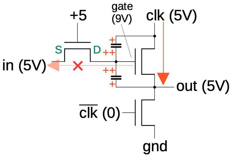
In the next step, the clock switches state and things become more interesting. The second transistor is on due to the voltage on the gate, so current flows from the clock to the output. In a "normal" circuit, the output would rise to 4 volts, losing a volt due to the threshold voltage of the second transistor. However, as the output voltage rises, it boosts the voltage on the gate capacitors and thus raises the gate voltage. The increased gate voltage allows the output voltage to rise above 4 volts, pushing the gate voltage even higher, until the output reaches 5 volts.10 Thus, the bootstrap driver produces a high-current output with the full 5 volts.

The second step in the operation of the bootstrap driver. As the output rises, it boosts the gate voltage even higher.

The second step in the operation of the bootstrap driver. As the output rises, it boosts the gate voltage even higher.

An important factor is that the first transistor now has a higher voltage on the right than on the left, so the source and drain switch roles. Since the transistor has 5 volts on the gate and on the (now) source, Vgs is 0 and current can't flow. Thus the first transistor blocks current flow from the gate, keeping the gate at its higher voltage. This is the critical role of the first transistor in the bootstrap driver, acting as a diode to block current flow out of the gate.

The diagram below shows what happens when the clock switches state again, assuming a low input. Now the first transistor's source voltage drops, making Vgs large and turning the transistor on. This allows the second transistor's gate voltage to flow out. Note that the first transistor is no longer acting as a diode, since current can flow in the "reverse" direction. The other important action in this clock phase is that the bottom transistor turns on, pulling the output low. These actions discharge the gate capacitance, preparing it for the next bootstrap cycle.

When the clock switches off, the driver is discharged, preparing it for the next cycle.

When the clock switches off, the driver is discharged, preparing it for the next cycle.

The 8086 die

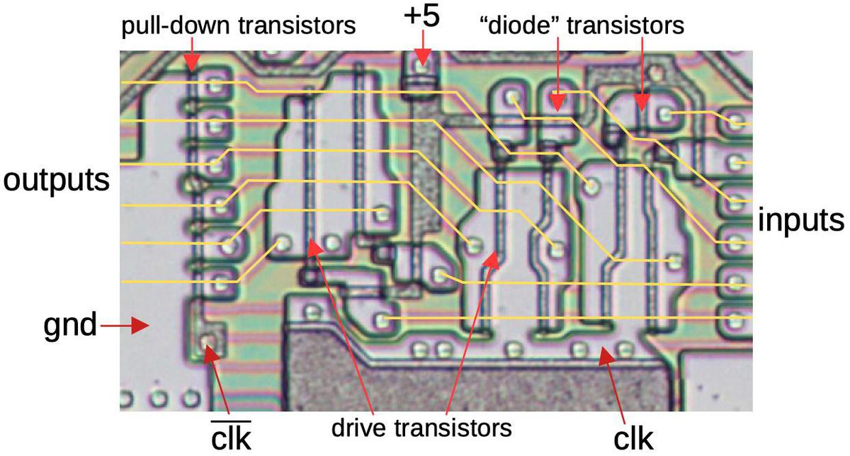
Now that I've explained the theory, how do bootstrap drivers appear on the silicon die of the 8086? The diagram below shows six drivers that control the ALU operation.11 There's a lot happening in this diagram, but I'll try to explain what's going on. For this photo, I removed the metal layer with acid to reveal the silicon underneath; the yellow lines show where the metal wiring was. The large pinkish regions are doped silicon, while the gray speckled lines are polysilicon on top. The greenish and reddish regions are undoped silicon, which doesn't conduct and can be ignored. A transistor is formed where a polysilicon line crosses silicon, with the source and drain on opposite sides. Note that some transistors share the source or drain region with a neighboring transistor, saving space. The circles are vias, connections between the metal and a lower layer.

Six bootstrap drivers as they appear on the chip.

Six bootstrap drivers as they appear on the chip.

The drivers start with six inputs at the right. Each input goes through a "diode" transistor with the gate tied to +5V. I've labeled two of these transistors and the other four are scattered around the image. Next, each signal goes to the gate of one of the drive transistors. These six large transistors pass the clock to the output when turned on. Note that the clock signal flows through large silicon regions, rather than "wires". Finally, each output has a pull-down transistor on the left, connecting it to ground (another large silicon region) under control of the inverted clock. The drive transistors are much larger than the other transistors, so they can provide much more current. Their size also provides the gate capacitance necessary for the operation of the bootstrap driver.

Although the six drivers in this diagram are electrically identical, each one has a different layout instead of repeating the same layout six times. This demonstrates how the layout has been optimized, moving transistors around to use space most efficiently.

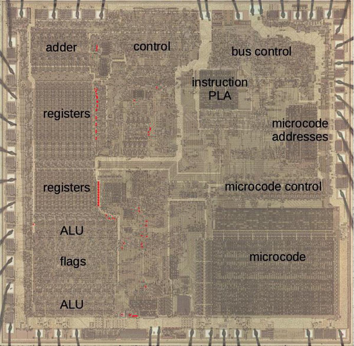
In total, the 8086 has 81 bootstrap drivers, mostly controlling the register file and the ALU (arithmetic-logic unit). The die photo below shows the location of the drivers, indicated with red dots. Most of them are in the center-left of the chip, between the registers and ALU on the left and the control circuitry in the center.

The 8086 die with main functional blocks labeled. The bootstrap drivers are indicated with red dots.

The 8086 die with main functional blocks labeled. The bootstrap drivers are indicated with red dots.

Conclusions

For the most part, the 8086 uses standard NMOS logic circuits. However, a few of its circuits are unusual, and the bootstrap driver is one of them. This driver is a tricky circuit, depending on some subtle characteristics of MOS transistors, so I hope my explanation made sense. This driver illustrates how Intel used complex, special-case circuitry when necessary to get as much performance from the chip as possible.

If you're interested in the 8086, I wrote about the 8086 die, its die shrink process and the 8086 registers earlier. I plan to write more about the 8086 so follow me on Twitter @kenshirriff or RSS for updates.

Notes and references

  1. Intel used a "bootstrap load" circuit in the 4004 and 8008 processors. The bootstrap load has many similarities to the bootstrap driver, using capacitance to boost the output voltage. But it is a different circuit, used in a different role. The bootstrap load was designed for PMOS circuits to boost the voltage from a pull-up transistor, using explicit capacitors, built with a process invented by Federico Faggin. I wrote about the bootstrap load here

  2. The only explanation of a bootstrap driver that I could find is in section 2.3.1 of DRAM Circuit Design: A Tutorial. The 8086 transistors with the gate wired to +5V puzzled me for the longest time. It seemed to me that this transistor would always be on, and thus had no function. However, the high voltage of the bootstrap driver gives it a function. I was randomly reading the DRAM book and suddenly recognized that one of the circuits in that book was similar to the mysterious 8086 circuit. 

  3. The threshold voltage was considerably higher for older PMOS transistors. To get around this, old chips used considerably higher supply voltages, so "losing" the threshold voltage wasn't as much of a problem. For instance, the Intel 4004 used a 15-volt supply. 

  4. The reason that MOSFETs are symmetrical in an integrated circuit and asymmetrical as physical components is that MOSFETs really have four terminals: source, gate, drain, and the substrate (the underlying silicon on which the transistor is constructed). In component MOSFETs, the substrate is internally connected to the source, so the transistor has three pins. However, the source-substrate connection creates a diode, making the component MOSFET asymmetrical. Four-terminal MOSFETs such as the 3N155 exist but are rare. The MOnSter 6502 made use of 4-terminal MOSFET modules to implement the 6502's pass transistors. 

  5. The load transistor is a special type of transistor, a depletion transistor that is doped differently. The doping produces a negative threshold voltage, so the transistor remains on and provides a relatively constant current. See Wikipedia for more on depletion loads. 

  6. The superbuffer has some similarity with a CMOS gate. Both use separate transistors to pull the signal high or low, with only one transistor on at a time. The difference is that CMOS uses a complementary transistor, i.e. PMOS, to pull the signal high. PMOS performs better in this role than NMOS. Moreover, a PMOS transistor is turned on by a 0 on the gate. This behavior eliminates the need for the inverter in a superbuffer. 

  7. The 8086 processor also uses completely different charge pumps to create a negative voltage for a substrate bias. I discuss that use of charge pumps here

  8. Why is it called a bootstrap driver? The term originates with footwear: boots often had boot straps on the top, physical straps to help pull the boots on. In the 1800s, the saying "No man can lift himself by his own boot straps" was used as a metaphor for the impossibility of improvement solely through one's own effort. (Pulling on the straps on your boots superficially seems like it should lift you off the ground, but is of course physically impossible.) By the mid-1940s, "bootstrap" was used in electronics to describe a circuit that started itself up through positive feedback, metaphorically pulling itself up by its bootstraps. The bootstrap driver continues this tradition, pulling itself up to a higher voltage. 

  9. Some circuits in the 8086 use physical capacitors on the die, constructed from a metal layer over silicon. The substrate bias generators use relatively large capacitors. There are also some small capacitors that appear to be used for timing reasons. 

  10. The exact voltage on the gate will depend on the relative capacitances of different parts of the circuit, but I'm ignoring these factors. The voltages that I show in the diagram are illustrations of the principle, not accurate values. 

  11. Some of the 8086's bootstrap drivers pre-discharge when the clock is low and produce an output when the clock is high, while other drivers operate on the opposite clock phases. The ALU drivers in the die photo operate on the opposite phases, but I've labeled the diagram to match the previous discussion.