The 8086 microprocessor was a groundbreaking processor introduced by Intel in 1978. It led to the x86 architecture that still dominates desktop and server computing. While reverse-engineering the 8086 from die photos, a particular circuit caught my eye because its physical layout on the die didn't match the surrounding circuitry. This circuit turns out to implement special functionality for a couple of instructions, subtlely changing the way they interacted with interrupts. Some web searching revealed that this behavior was changed by Intel in 1978 to fix a problem with early versions of the 8086 chip. By studying the die, we can get an idea of how Intel dealt with bugs in the 8086 microprocessor.
In modern CPUs, bugs can often be fixed through a microcode patch that updates the CPU during boot.1 However, prior to the Pentium Pro (1995), microprocessors could only be fixed through a change to the design that fixed the silicon. This became a big problem for Intel with the famous Pentium floating-point division bug. The chip turned out to have a bug that resulted in rare but serious errors when dividing. Intel recalled the defective processors in 1994 and replaced them, at a cost of $475 million.
The circuit on the die
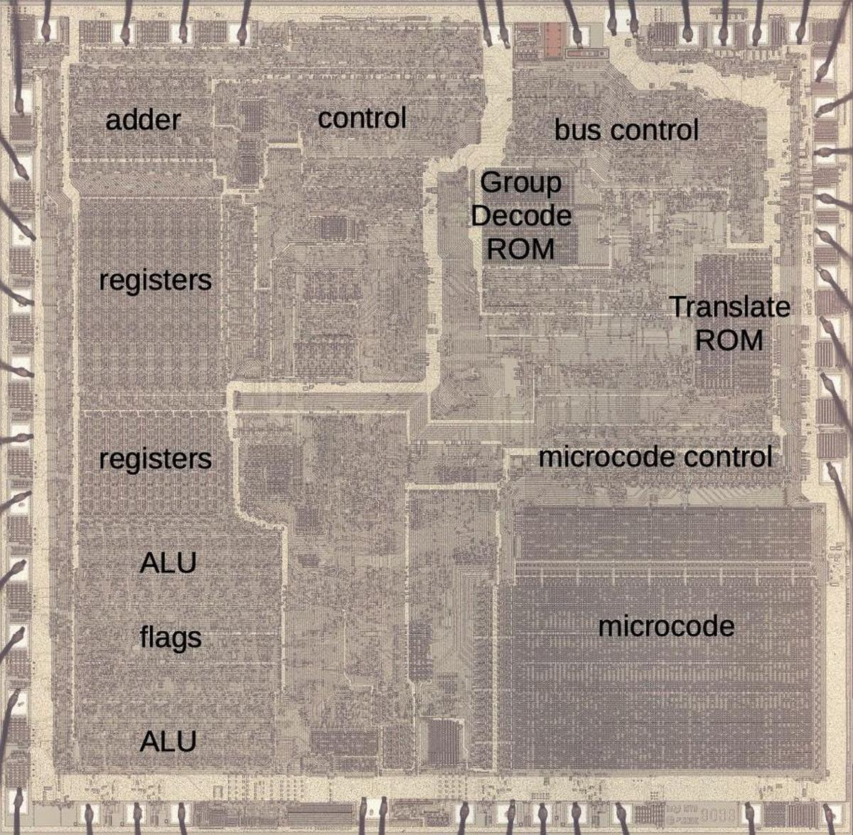
The microscope photo below shows the 8086 die with the main functional blocks labeled. This photo shows the metal layer on top of the silicon. While modern chips can have more than a dozen layers of metal, the 8086 has a single layer. Even so, the metal mostly obscures the underlying silicon. Around the outside of the die, you can see the bond wires that connect pads on the chip to the 40 external pins.
The relevant part of the chip is the Group Decode ROM in the upper center. The purpose of this circuit is to categorize instructions into groups that control how they are decoded and processed. For instance, very simple instructions (such as setting a flag) can be performed directly in one cycle. Other instructions are not complete instructions, but a prefix that modifies the following instruction. The remainder of the instructions are implemented in microcode, which is stored in the lower-right corner of the chip. Many of these instructions have a second byte, the "Mod R/M" byte that specifies a register and the memory addressing scheme. Some instructions have two versions: one for an 8-bit operand and one for a 16-bit operand. Some operations have a bit to swap the source and destination. The Group Decode ROM is responsible for looking at the 8 bits of the instruction and deciding which groups the instruction falls into.
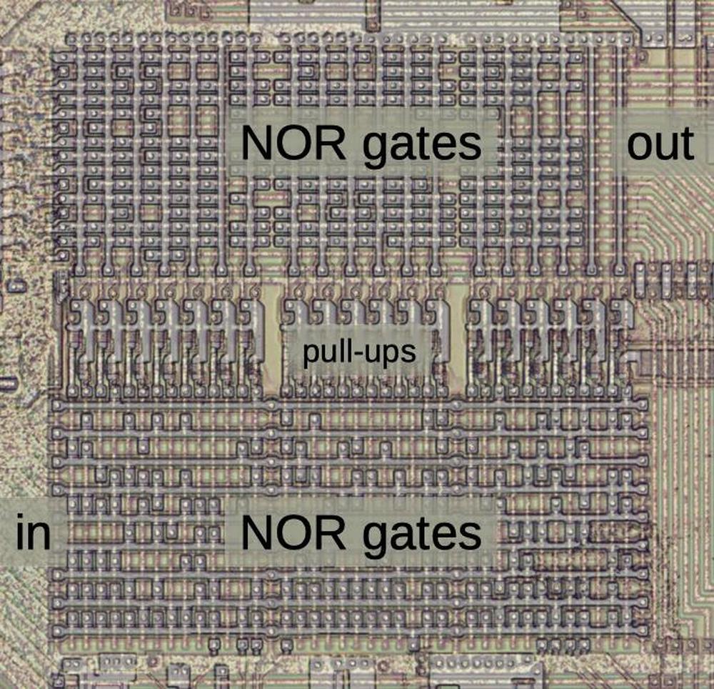
The photo above shows the Group Decode ROM in more detail. Strictly speaking, the Group Decode ROM is more of a PLA (Programmable Logic Array) than a ROM, but Intel calls it a ROM. It is a regular grid of logic, allowing gates to be packed together densely. The lower half consists of NOR gates that match various instruction patterns. The instruction bits are fed horizontally from the left, and each NOR gate is arranged vertically. The outputs from these NOR gates feed into a set of horizontal NOR gates in the upper half, combining signals from the lower half to produce the group outputs. These NOR gates have vertical inputs and horizontal outputs.
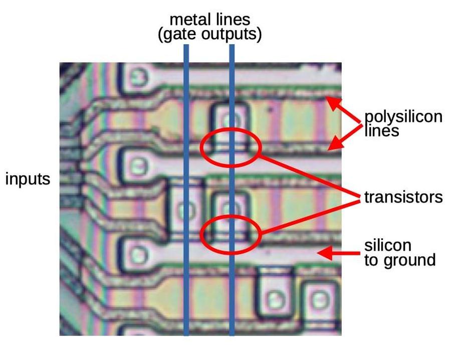
The diagram below is a closeup of the Group Decode ROM, showing how the NOR gates are constructed. The pinkish regions are silicon, doped with impurities to make it a semiconductor. The gray horizontal lines are polysilicon, a special type of silicon on top. Where a polysilicon crosses conductive silicon, it forms a transistor. The transistors are wired together by metal wiring on top. (I dissolved the metal layer with acid to show the silicon; the blue lines show where two of the metal wires were.) When an input is high, it turns on the corresponding transistors, pulling the vertical lines low. This creates NOR gates with multiple inputs. The key idea of the PLA is that at each point where horizontal and vertical lines cross, a transistor can be present or absent, to select the desired gate inputs. By doping the silicon in the desired pattern, transistors can be created or omitted as needed. In the diagram below, two of the transistors are highlighted. You can see that some of the other locations have transistors, while others do not. Thus, the PLA provides a dense, flexible way to produce a set of outputs from a set of inputs.
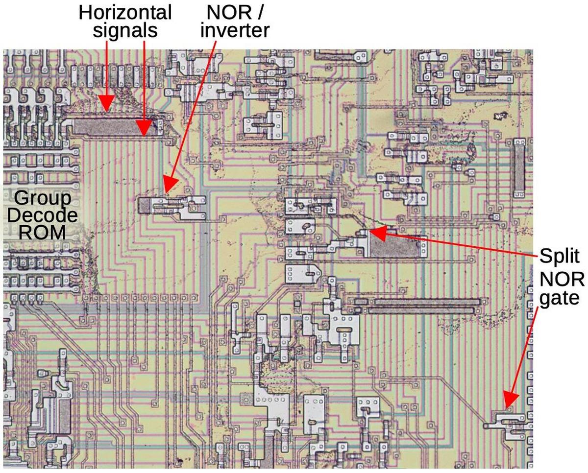
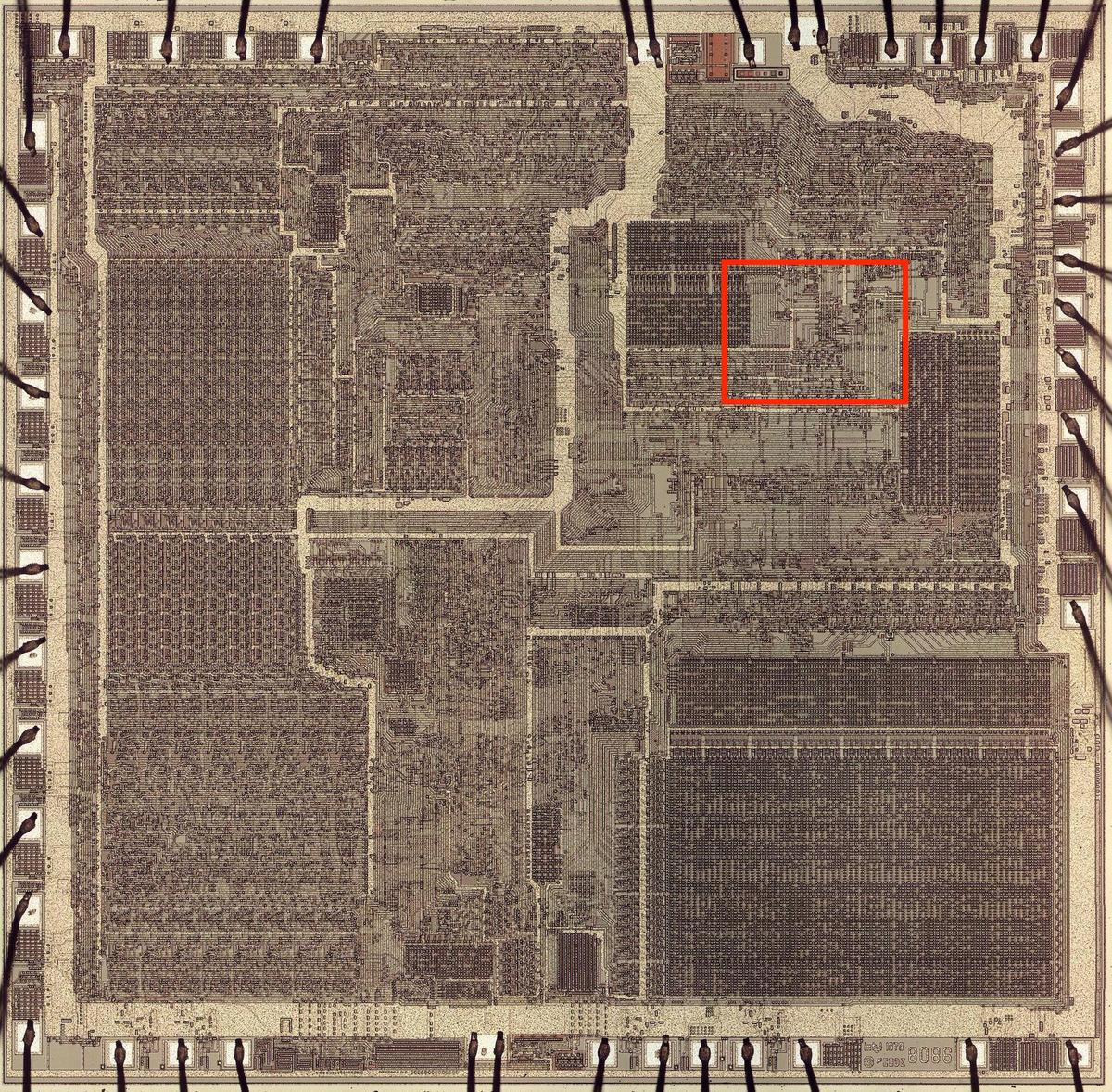
Zooming out a bit, the PLA is connected to some unusual circuitry, shown below. The last two columns in the PLA are a bit peculiar. The upper half is unused. Instead, two signals leave the side of the PLA horizontally and bypass the top of the PLA. These signals go to a NOR gate and an inverter that are kind of in the middle of nowhere, separated from the rest of the logic. The output from these gates goes to a three-input NOR gate, which is curiously split into two pieces. The lower part is a normal two-input NOR gate, but then the transistor for the third input (the one we're looking at) is some distance away. It's unusual for a gate to be split across a distance like this.
It can be hard to keep track of the scale of these diagrams. The highlighted box in the image below corresponds to the region above. As you can see, the circuit under discussion spans a fairly large fraction of the die.
My next question was what instructions were affected by this mystery circuitry.
By looking at the transistor pattern in the Group Decode ROM, I determined that the two curious columns matched instructions with bits
10001110 and 000xx111.
A look at the 8086 reference shows that the first bit pattern corresponds to the instructions MOV sr,xxx, which loads a value into a segment register.
The second bit pattern corresponds to the instructions POP sr, which pops a value from the stack into a segment register.
But why did these instructions need special handling?
The interrupt bug
After searching for information on these instructions, I came across errata stating: "Interrupts Following MOV SS,xxx and POP SS Instructions May Corrupt Memory. On early Intel 8088 processors (marked “INTEL ‘78” or “(C) 1978”), if an interrupt occurs immediately after a MOV SS,xxx or POP SS instruction, data may be pushed using an incorrect stack address, resulting in memory corruption." The fix to this bug turns out to be the mystery circuitry.
I'll give a bit of background. The 8086, like most processors, has an interrupt feature where an external signal, such as a timer or input/output, can interrupt the current program. The processor starts running different code to handle the interrupt, and then returns to the original program, continuing where it left off. When interrupted, the processor uses its stack in memory to keep track of what it was doing in the original program so it can continue. The stack pointer (SP) is a register that keeps track of where the stack is in memory.
A complication is that the 8086 uses "segmented memory", where memory is divided into chunks (segments) with different purposes. On the 8086, there are four segments: the Code Segment, Data Segment, Stack Segment, and Extra Segment. Each segment has an associated segment register that holds the starting memory address for that segment. Suppose you want to change the location of the stack in memory, maybe because you're starting a new program. You need to change the Stack Segment register (called SS) to point to the new location for the stack segment. And you also need to change the Stack Pointer register (SP) to point to the stack's current position within the stack segment.
A problem arises if the processor receives an interrupt after the Stack Segment register has been changed, but before
the Stack Pointer register has been changed.
The processor will store information on the stack using the old stack pointer address but in the new segment.
Thus, the information is stored into essentially a
random location in memory, which is bad.2
Intel's fix was to delay an interrupt after an update to the stack segment register, so you had a chance to update the stack pointer.3
The stack segment register could be changed in two ways.
First, you could move a value to the register ("MOV SS, xxx" in assembly language), or you could pop a value off the stack
into the stack segment register ("POP SS").
These are the two instructions affected by the mystery circuitry.
Thus, we can see that Intel added circuitry to
delay an interrupt immediately after one of these instructions and avoid the bug.
Conclusions
One of the interesting things about reverse-engineering the 8086 is when I find a curious feature on the die and then find that it matches an obscure part of the 8086 documentation. Most of these are deliberate design decisions, but they show how complex and ad-hoc the 8086 architecture is, with many special cases. Each of these cases results in some circuitry and gates, complicating the chip. (In comparison, I've reverse-engineered the ARM1 processor, a RISC processor that started the ARM architecture. The ARM1 has a much simpler architecture with very few corner cases. This is reflected in circuitry that is much simpler.)
The case of the segment registers and interrupts, however, is the first circuit that I've found on the 8086 die that is part of a bug fix. This fix appears to have been fairly tricky, with multiple gates scattered in unused parts of the chip. It would be interesting to get a die photo of a very early 8086 chip, prior to this bug fix, to confirm the change and see if anything else was modified.
If you're interested in the 8086, I wrote about the 8086 die, its die shrink process and the 8086 registers earlier. I plan to write more about the 8086 so follow me on Twitter @kenshirriff or RSS for updates. I've also started experimenting with Mastodon recently as @[email protected].
Notes and references
-
The modern microcode update process is more complicated than I expected with updates possible before the BIOS is involved, during boot, or even while applications are running. Intel provides details here. Apparently Intel originally added patchable microcode to the Pentium Pro for chip debugging and testing, but realized that it would be a useful feature to fix bugs in the field (details). ↩
-
The obvious workaround for this problem is to disable interrupts while you're changing the Stack Segment register, and then turn interrupts back on when you're done. This is the standard way to prevent interrupts from happening at a "bad time". The problem is that the 8086 (like most microprocessors) has a non-maskable interrupt (NMI), an interrupt for very important things that can't be disabled. ↩
-
Intel documents the behavior in a footnote on page 2-24 of the User's Manual:
There are a few cases in which an interrupt request is not recognized until after the following instruction. Repeat, LOCK and segment override prefixes are considered "part of" the instructions they prefix; no interrupt is recognized between execution of a prefix and an instruction. A MOV (move) to segment register instruction and a POP segment register instruction are treated similarly: no interrupt is recognized until after the following instruction. This mechanism protects a program that is changing to a new stack (by updating SS and SP). If an interrupt were recognized after SS had been changed, but before SP had been altered, the processor would push the flags, CS and IP into the wrong area of memory. It follows from this that whenever a segment register and another value must be updated together, the segment register should be changed first, followed immediately by the instruction that changes the other value. There are also two cases, WAIT and repeated string instructions, where an interrupt request is recognized in the middle of an instruction. In these cases, interrupts are accepted after any completed primitive operation or wait test cycle.
Curiously, the fix on the chip is unnecessarily broad: a
MOVorPOPfor any segment register delays interrupts. There was no hardware reason for this: the structure of the PLA means that all the necessary instruction bits were present and it would be no harder to test for the Stack Segment register specifically. The fix of delaying interrupts after a POP or MOV remains in the x86 architecture today. However, it has been cleaned up so only instructions affecting the Stack Segment register cause the delay; operations on other segment registers have no effect. ↩
12 comments:
After Wikipedia: "8086... It was an attempt to draw attention from the less-delayed 16-bit and 32-bit processors of other manufacturers — Motorola, Zilog, and National Semiconductor.". Really groundbreaking! Stop-gap measure to avoid Intel having their ar.es handed in.
The immediate question that comes to my mind - is there any way to run these instructions forever, back-to-back? Can this cause you to never be able to service NMIs at all?
(For that matter - are there other ways of not being able to service NMIs? I don't know the 8086 that well.)
This also reminds me of branch delay slots in an odd way, as well as ARM's games with a few of the coprocessor registers - there are a couple that are architecturally _mandated_ not to take effect immediately, so you can change them atomically.
There is another blogger that used the 8086 die photo you posted two years ago to do an analysis of the internal Microcode ROM, which is very likely that you're already aware of:
https://www.reenigne.org/blog/8086-microcode-disassembled/
The analysis relied on an Intel patent that documents some of the 8086 internal Microcode to reverse engineer it and fully document how the Microcode program itself is supposed to work. Doing so, he found that there were some notorious differences involving interrupt handling in the actual implementation as found in the Processor (Based on what you decapped) compared to what was stated in the patent, which suffered from a stall bug in some obscure circunstance.
I recall that when casually doing digital archaeology, I found a magazine talking about the IBM PC mentioning than the early 8086 units had a major bug that could cause an "interrupt storm", but to not worry about it cause the IBM PC used later, fixed Processors (Albeit it uses an 8088, not 8086). I did commented his blog to mention than his Microcode analysis was using as base an 8086-2 and not the original 8086, so it is possible than the differences in internal Microcode were precisely because he was seeing the fixed version, and that is still possible than the original 8086 is an exact match of the patent cause the bug he described happened there.
So yes, I'm also interesed in seeing an early 8086 decap and analysis if you manage to get an unit for some destructive testing, mostly to see how the bugfixes themselves are implemented and how big of a variation there is between minor Revisions/Steppings of what is otherwise the "same" Processor. Developers programming accurate emulators (Like the MAME guys) are obsessed with the extremely specific details and high quality info about those isn't easy to come by. I expect than at some point those projects would end up emulating one or multiple silicon Revisions of the same chip to account for the different bugs/erratas.
On Intel it's not possible. However, look up "Cyrix coma bug" for a case where it was possible to run uninterruptible instructions forever and hang the PC.
Aaargh. Segments. I remember Les Vadasz telling me there were good reasons for it. Do you know what the architectural thinking is behind it? Does it actually save transistors?
Wasn't the segmentation purely the easy way to use 1MB physical memory with 16bit addresses?
As well as allowing access to a full 1MB, it also helps memory management. The full address is computed with 'segment << 8 + offset', this means chunks of data up to 64KB can be relocated to any one of 1MB / 2^8 = 64K locations in memory by just making sure the appropriate segment value is in use. For example, if your program was less than 64KB (not uncommon at the time) it could be located at any CS (Code Segment) the OS chooses.
It is a known bug, but it is interesting to see how the fix was implemented... It is literally a patch! :)
It should be noted that 8088 disables interrupts after any POP sr or MOV sr,reg instruction, not only for POP SS and MOV SS,reg. That it a good way to detect if you have a buggy CPU in the software - setup an INT 1 (trace) handler, and set the TF (trace flag), and then run POP ES or POP DS, and see if your handler gets executed right after this or not - if it is, you have a buggy CPU.
Now that you've researched NMOS 8086/8088, it would be interesting to see the CMOS variants.
It appears that there are at least two different CMOS implementations: Harris (later Intersil, now Renesas, apparently still being manufactured), and OKI.
Interestingly enough early "Intel" marked 80C88 were manufactured by OKI (have the same package, made in Japan), while later ones (in a more conventional Intel package) appear to be manufactured using Harris design.
Other than difference in packages, there is at least one difference in behavior, related to this MOV SS,reg/POP SS bug - For some reason the Harris design also disables interrupts following PUSH sr instructions...
Did you make a full die-shot with the metal layer removed and the polysilicon intact? or did you only create pictures of the parts analyzed?
One source of an "early" 8086 would be from the IBM Displaywriter, introduced in June 1980 with a 5MHz 8086 - Let me see what I can dig up.
One source of an "early" 8086 would be from the IBM Displaywriter, introduced in June 1980 with a 5MHz 8086 - Let me see what I can dig up.
was this used in Space Shuttles also? was it the prefetch queue?
Post a Comment