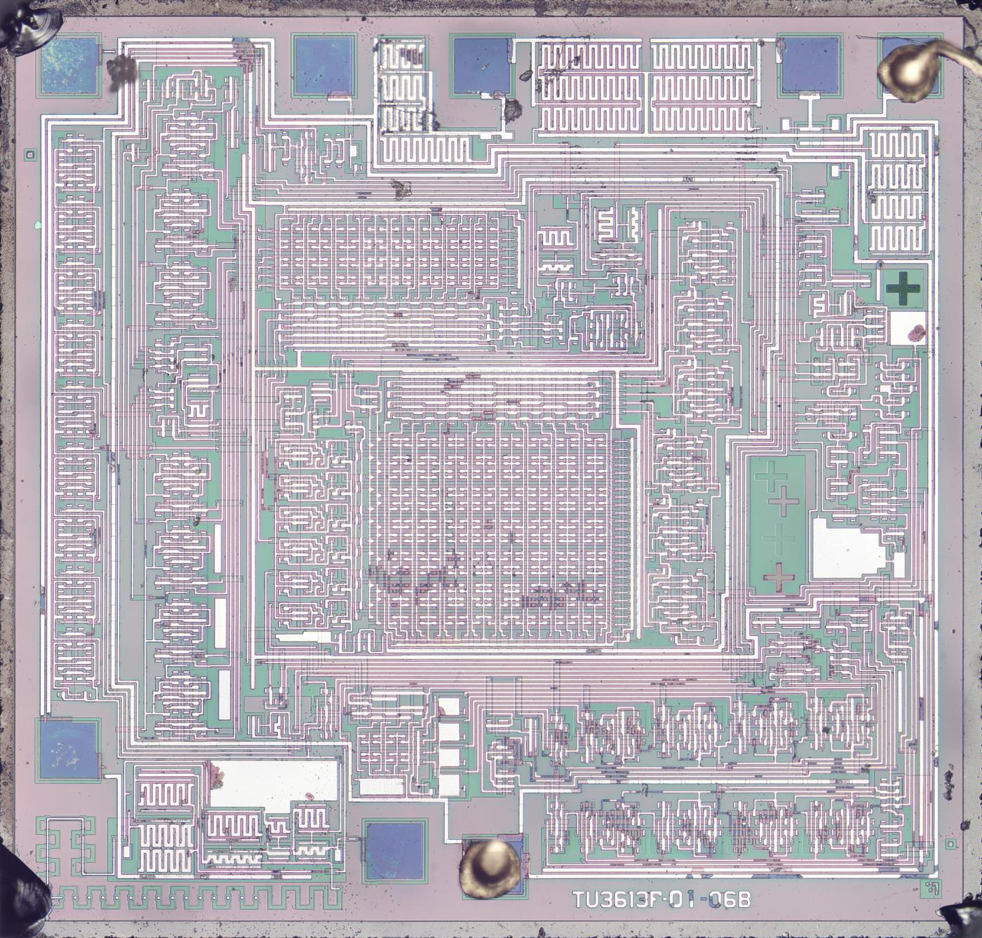
For the holidays, I decapped a chip that plays three Christmas melodies. The UM66T melody chip from the 1980s was designed for applications such as greeting cards and toys. It looks like a transistor, but when connected to a battery and speaker it plays music. The die photo below shows the tiny silicon chip that I reverse engineer in this blog post.
The video below shows the chip in action. Click to hear the chip play Jingle Bells, Santa Claus is Coming to Town, and We Wish You a Merry Christmas.
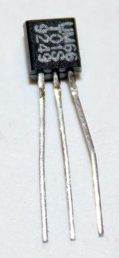
The chip is packaged in a 3-pin package that looks like a transistor (below). I dissolved the epoxy package in boiling sulfuric acid to expose the silicon die inside. This was my first acid decap and it turned out okay, although there are some scratches on the die. The composite photo above shows the CMOS chip under the microscope. The features are fairly large, even for the time; the metal traces are about 3.3µm wide and the silicon about 5.4µm.
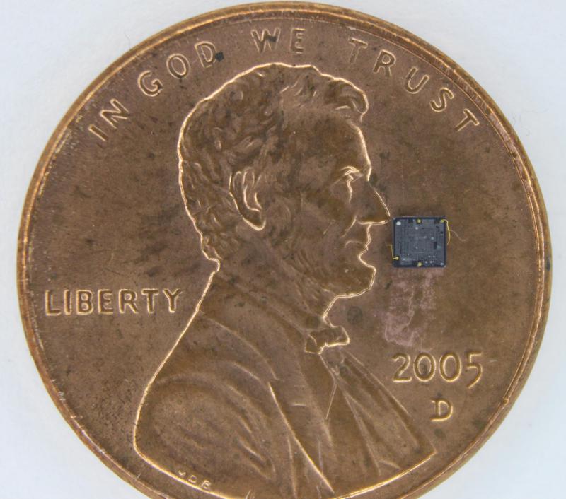
The silicon die is very small, about 1.8mm×1.8mm. The photo below gives an idea of the scale.
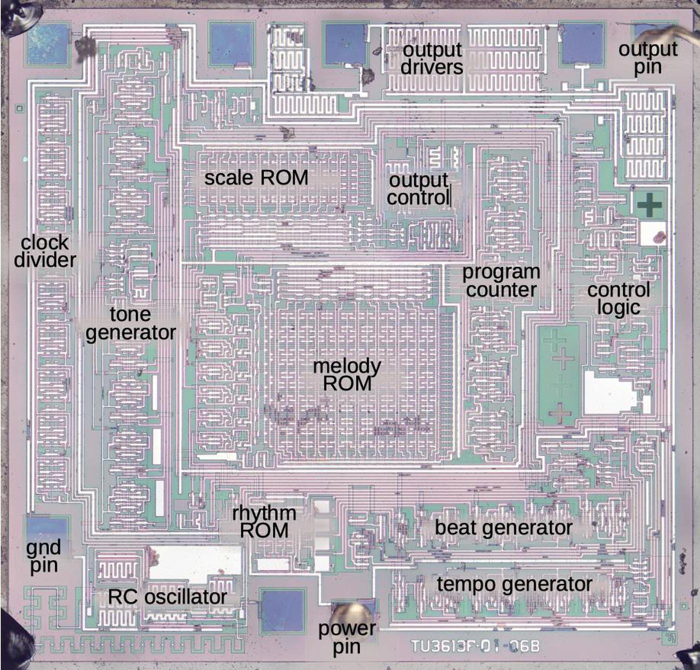
I've labeled the die photo with the functional blocks. The melody chip is an optimized, minimal design. It is constructed from flip-flops and gates, not the microcontroller you might expect.
The chip has 3 pins, but there are 8 pads on the die. The other pins appear to be used for testing. By activating one of the pins, the chip can be put into a test mode. The test mode runs through the songs at 512× speed so the chip can be tested quickly without waiting for the tunes to play. The other test pins appear to expose other internal data for testing.
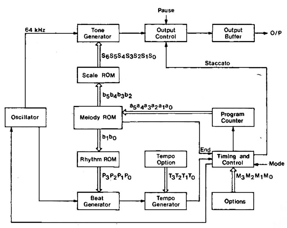
The block diagram below shows the structure of the chip. (Inconveniently, I didn't get this diagram until after I'd reverse-engineered the circuitry.) The basic idea is that the "program counter" steps through the 64 notes stored in the melody ROM. Four bits form the note pitch index, while two bits select the note duration. The Scale ROM and tone generator are used to convert the pitch index into the desired output tone. Meanwhile, the Rhythm ROM converts the 2-bit note duration into a 4-bit value indicating how long the note is.
The chip is built from CMOS, like most modern ICs. The photo below shows an inverter: a PMOS transistor on the left and an NMOS transistor on the right. The PMOS one turns on with a 0 input, pulling the output high. The NMOS transistor turns on with a 1, pulling the output low. Thus, the two transistors implement the desired inverter behavior.
The melody ROM
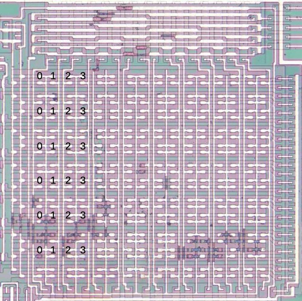
The 64 notes are stored in a 64×6 ROM, shown below. Each note is 4 bits for the frequency and 2 bits for the duration of the note. The ovals are the transistor gates; bits are stored in the wiring pattern of the transistors, either to the left or to the right. The vertical column select lines from the top select one column in the ROM. The vertical lines from the bottom, however, inactivate the transistor.
Physically, the ROM stores four notes in each column, so it has 16 columns of 24 bits. At the top of the ROM is a binary decoder that energizes one of the 16 columns, based on the input value. The transistors at the left of the ROM select one bit out of each four to produce the desired 6-bit word. The 6 bits are latched. Then 4 bits are used to generate the desired note frequency, while two bits select the duration of the note (half note, quarter note, or eighth note).
In the diagram above, the numbers show the locations of the first four words. The first word is 000100, a start code. The next two words are 011100; 0111 indicates the note E5 and 00 indicates a short duration.1 The next word is by 011101, indicating a longer E5. Thus, the indicated words store the first three notes of "Jingle Bells".
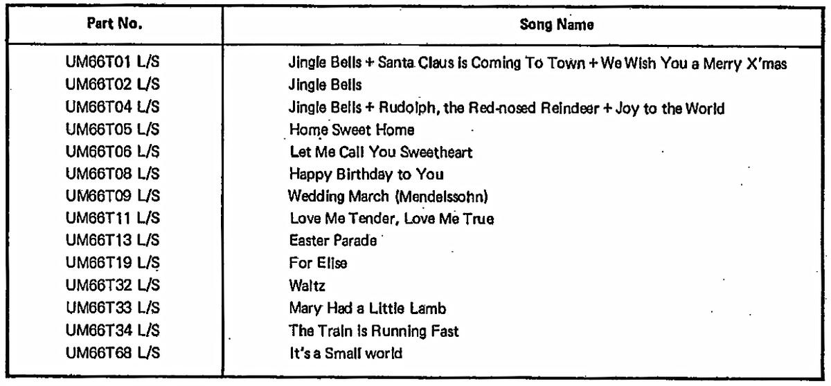
The metal layer of an IC can be changed relatively easily. By changing the metal layer, different versions of the chip could be manufactured with different ROMs, producing different songs. (The chip could also be manufactured with different note ranges, tempo, and beats, providing more flexibility.) The table below shows the songs that were available.2
Generating the note frequency
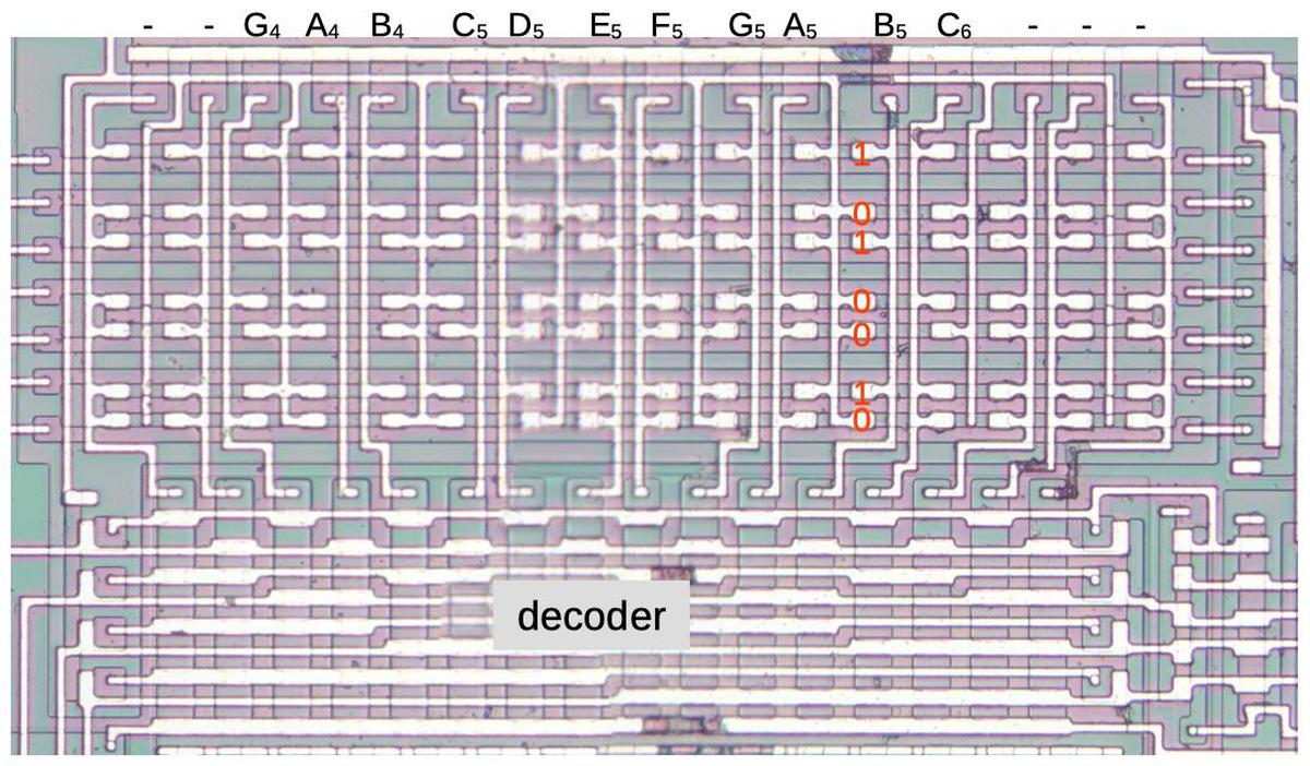
The melody ROM doesn't specify the note's frequency directly, but instead has a value from 0 to 15. A second ROM, the scale ROM, has the mapping to convert the note value into a frequency. Specifically, the output frequency is 32768÷N, where N is the value in the scale ROM. The frequency resolution from this isn't great, so some notes are noticeably out of tune, but it's good enough for this application.
The image above shows the scale ROM, configured to produce the notes G4 through C6 in the key of C. (Different versions of the chip can generate different notes by changing the scale ROM.) As with the melody ROM, the binary values are generated by the wiring of the metal layer to the transistors. For instance, the note B5 has the bits 0,1,0,0,1,0,1 (from bottom to top). Below the ROM, the decoder activates one of the 16 column lines based on the 4-bit note value. (Notice the binary pattern of transistors in the decoder: the top rows alternate, the next rows are every 2, then every 4 and every 8.
The chip uses an unusual technique to generate the output frequency. The standard way is to divide the clock frequency by the scale factor with a counter, but instead the chip has an unusual approach to save a few transistors. It uses a 7-bit linear-feedback shift register. The construction of the linear-feedback shift register is that the input is the XOR of the last two bits. It will cycle pseudo-randomly through all 127 values.4
The trick in the melody chip is to initialize the shift register with a particular value loaded from the ROM, and run through the sequence until the value 1000000 is reached. By picking the right starting value, the desired number of counts will be obtained. The diagram below illustrates the operation of the shift register with the B5 input 0100101. With this starting value, it takes 34 steps to reach the final value of binary 1000000. Notice how the bits are shifted to the right each step, with a new bit inserted at the left.
0 1 0 0 1 0 1
1 0 1 0 0 1 0
1 1 0 1 0 0 1
1 1 1 0 1 0 0
0 1 1 1 0 1 0
1 0 1 1 1 0 1
1 1 0 1 1 1 0
1 1 1 0 1 1 1
0 1 1 1 0 1 1
0 0 1 1 1 0 1
1 0 0 1 1 1 0
1 1 0 0 1 1 1
0 1 1 0 0 1 1
0 0 1 1 0 0 1
1 0 0 1 1 0 0
0 1 0 0 1 1 0
1 0 1 0 0 1 1
0 1 0 1 0 0 1
1 0 1 0 1 0 0
0 1 0 1 0 1 0
1 0 1 0 1 0 1
1 1 0 1 0 1 0
1 1 1 0 1 0 1
1 1 1 1 0 1 0
1 1 1 1 1 0 1
1 1 1 1 1 1 0
1 1 1 1 1 1 1
0 1 1 1 1 1 1
0 0 1 1 1 1 1
0 0 0 1 1 1 1
0 0 0 0 1 1 1
0 0 0 0 0 1 1
0 0 0 0 0 0 1
1 0 0 0 0 0 0
Since this takes 34 steps, the clock frequency is divided by 34 and the output frequency is 32768 ÷ 34 = 963 Hertz, close to the desired frequency of 997 Hertz.3 For another example, G4 starts with 1001010 and runs for 84 counts, yielding a frequency of 392 Hertz. Thus, the ROM controls the frequency of the notes produced. Note that the starting values are not obviously correlated with the frequency; they depend on the sequence generated by the linear feedback shift register. (This sequence is called pseudo-random since it is deterministic but appears kind of random.)
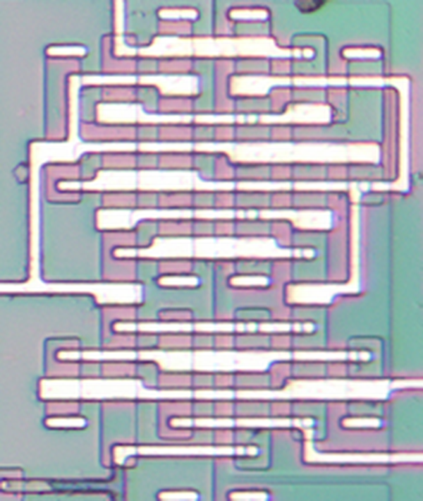
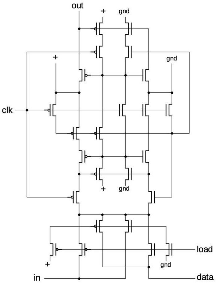
Next, I'll discuss the implementation of the shift register. The die photo below shows one stage of the shift register. It receives input from the stage below and passes its output to the stage above. The stage is constructed from 26 transistors: 13 PMOS transistors on the left and 13 NMOS transistors on the right. The transistors are oriented vertically along the pink regions of doped silicon. The transistor gates are where the metal lines widen. Note that transistors in a column are connected by the silicon.
The schematic below shows how the transistors are connected, corresponding to the die photo above.
At a slightly higher level, the circuit consists of inverters and multiplexers5 as shown below. Each loop of two inverters holds a bit. The first multiplexer selects the input: either a value from the ROM that is loaded into the shift register, or the value from the previous stage. When the clock goes high, this value is loaded into the first inverter loop. When the clock goes low, the value in the first inverter loop is transferred to the second inverter loop, and thus the output. Thus, it takes one complete clock cycle (low then high) to shift a bit one stage in the shift register.
The clock
The chip runs on a 64-kilohertz clock. This clock is generated from a simple resistor-capacitor-inverter oscillator inside the chip, avoiding the need for external components. Because the capacitor takes some time to charge through the resistor, the oscillation speed is controlled.
The die photo below shows a closeup of the oscillator. The white rectangle is the capacitor. The green zig-zag is the resistor. Note that the resistance can be adjusted by shorting out part of the resistor in the metal layer. The white zig zags are the gates of the inverter transistors. These transistors are larger than the typical logic transistors.
The on-chip R-C oscillator is cheap but inaccurate, unlike a quartz crystal oscillator. If the voltage changes, the frequency changes. In the video below, I lower and raise the voltage, and you can hear the effect on the tunes as the frequency changes.
Timing
The 64-kilohertz clock goes through a divider chain to divide the frequency by 512. This divider is made of nine toggle flip-flops, each one dividing the frequency by 2. These flip-flops are built from inverters and multiplexers similar to the shift register flip-flops, but wired to toggle. This feeds the beat generator, which adjusts the timing for quarter notes, eighth notes, etc. It uses a linear-feedback shift register, similar to the tone generator, but with four shift register stages. The shift register is loaded with a value from the rhythm ROM that determines the length of the note.
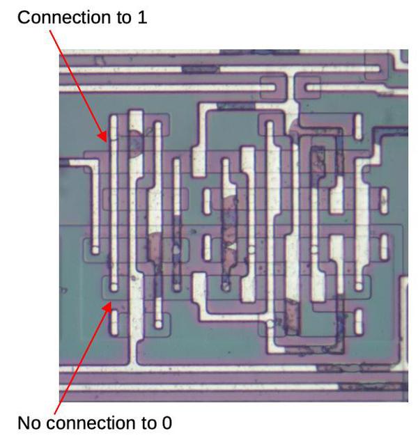
The output from the beat generator goes to the tempo generator, which divides its input by a preset amount (1 to 15) to generate a tempo between 128 and 1920 beats per minute. The tempo generator is also a 4-bit linear feedback shift register. The input to the shift register is hard wired to set the fixed tempo. The photo below shows one stage, wired to 1. A small change to the metal layer would cause 0 to be connected instead of 1.
The program counter counts through the 64 notes, providing the address to the melody ROM. It is built from toggle flip-flops chained together to build a 6-bit counter. The flip-flops have a reset line to initialize the counter to 0 at the start. The chip has a few dozen logic gates to keep track of the current state, handle startup, test mode, and so forth.
Conclusion
This melody chip uses simple circuits to produce songs in a flexible way. The chip integrates all the necessary circuitry including the R-C oscillator, so only a battery and a speaker were required. Nowadays a microcontroller would be the easiest way to implement this. This 1980s chip, however, uses small ROMs and simple counters to produce the tunes. I'll end with a quote from John Nolan: "Nothing says 'Christmas' like decapitating a microchip that plays slightly off-key Christmas songs."
This article is the extension of my earlier Twitter thread, which had a bunch of discussion on Hacker News. I announce my latest blog posts on Twitter, so follow me @kenshirriff. I also have an RSS feed. Thanks to Mark Fraser for finding an article on the chip.6
Notes and references
-
The note codes range from 0010 for G4 through 1100 for C6, in the key of C. I wrote a short Python program to convert the ROM contents to notes. ↩
-
Datasheets for the UM66T are available here, here, and here. A die photo of a different UM66T version is on siliconpr0n; I think this one plays Für Elise. ↩
-
The output frequency is half what you might expect from the 64 kHz clock. To keep the waveform symmetrical, there is a toggle flip-flop on the output that divides the counter output by 2. ↩
-
The 7-bit LFSR has 127 values instead of 128 values because it will get stuck in the all-zero value (since 0⊕0 = 0). ↩
-
The multiplexers are built from a CMOS circuit called a transmission gate (below). A transmission gate operates as a switch. When enable is high, both transistors turn on, passing the signal through the gate. When enable is low, both transistors turn off, blocking the signal. (Note that the PMOS transistor has an inverted control signal.) A multiplexer is built from two transmission gates. The control signal is connected to the two transmission gates with opposite polarity, so one transmission gate will be active at a time. Thus, one of the inputs is selected.
Schematic of a transmission gate. -
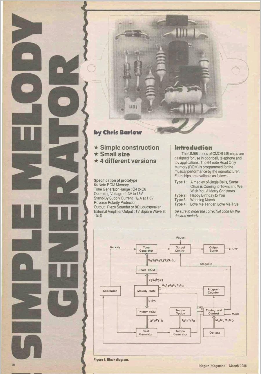
A 1988 article (p24-26) in Maplin Electronics described how to build a circuit with the UM66T.
First page of the article from Maplin Electronics, March 1988.




10 comments:
You had me at 'boiling sulphuric acid'.
That device is an absolutely beautiful piece of vintage tech.
My first thought was a counter generating an address to a ROM, with the data going to a DAC. Oh, I’m guessing that chip might be 10X the size, don’t want to think about the cost. I’m sure that the designers knew a lot more about music than I do, designing the chip at a very high music level.
The second video encapsulates the spirit of Christmas 2021 perfectly.
Hi Ken,
There are some double phrases in the note frequency example paragraph.
I'm surprised it uses an LFSR but at the same time had a bot of an a-ha moment. They could have used the LFSR too for the program counter, if 15 lines of music was enough. What's your theory about why this isn't used more often in other (computer) chips with linearly stepped ROMs (that don't need random-access)?
Mark: I've seen very early microcontrollers that use an LFSR for the program counter (and shuffle the ROM accordingly). My theory is that this was abandoned mostly because it makes design and debugging much harder, since the ROM is out of order. Also, an LFSR can't access location 0, so you lose one location. As transistors became cheaper, it wasn't worth the optimization of using an LFSR.
26 transistors for a shift register stage seems quite a lot, especially compared to the over all slimmed design. I feel that I've seen much more compact shift registers in some of your other posts, but I guess that those weren't fully static designs. On the other hand, shift registers still seem to take up a pretty modest part of the area (I think?), so maybe it doesn't matter so much.
Interesting to hear about the consistent use of LFSRs for clock division!
I remember those. I got Fur Elise for my 8th birthday and it was one of my greatest treasures. I remember it going off key whenever battery was not connected correctly (although not dying, I don't remember replacing battery like ever).
I am thinking how many transistors are actually saved by using scale ROM. Well the saving is 3 x 64 = 192 transistors in melody ROM. On the other hand scale ROM itself has 16 x 7 = 112 transistors. But if I add only 16 4-input NAND or NOR in decode logic, 8 transistors for each, I have to add additional 128 transistors. Now I already have 192 saved transistors vs 240 additional and I ignore rest of the additional logic needed. Not mentioning less regular design and lower transistor density. It seems there was no saving at all.
I think it's 24 transistors in the shift register stage-? I'm very new to electronics, but studying the two schematics, I think it's clever how in the first loop, two transistors logically combine inversion of the output with a transmission gate enabled by the clock, saving two transistors. Love the blog, thanks for all the fascinating posts!
Post a Comment