Intel's 386 processor (1985) was an important advance in the x86 architecture, not only moving to a 32-bit processor but also switching to a CMOS implementation. I've been reverse-engineering parts of the 386 chip and came across two interesting and completely different circuits that the 386 uses to implement an XOR gate: one uses standard-cell logic while the other uses pass-transistor logic. In this article, I take a look at those circuits.
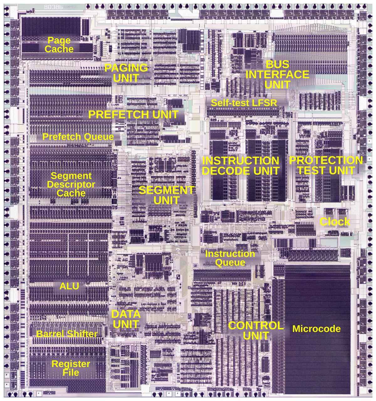
The die photo above shows the two metal layers of the 386 die. The polysilicon and silicon layers underneath are mostly hidden by the metal. The black dots around the edges are the bond wires connecting the die to the external pins. The 386 is a complicated chip with 285,000 transistor sites. I've labeled the main functional blocks. The datapath in the lower left does the actual computations, controlled by the microcode ROM in the lower right.
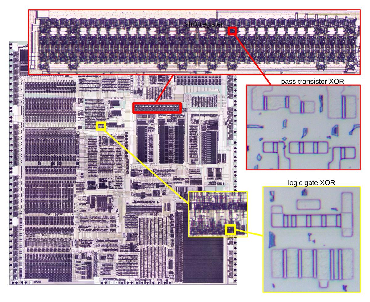
Despite the complexity of the 386, if you zoom in enough, you can see individual XOR gates. The red rectangle at the top (below) is a shift register for the chip's self-test. Zooming in again shows the silicon for an XOR gate implemented with pass transistors. The purple outlines reveal active silicon regions, while the stripes are transistor gates. The yellow rectangle zooms in on part of the standard-cell logic that controls the prefetch queue. The closeup shows the silicon for an XOR gate implemented with two logic gates. Counting the stripes shows that the first XOR gate is implemented with 8 transistors while the second uses 10 transistors. I'll explain below how these transistors are connected to form the XOR gates.
A brief introduction to CMOS
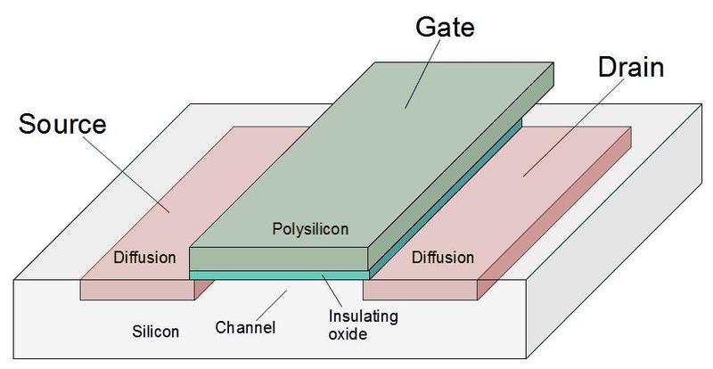
CMOS circuits are used in almost all modern processors. These circuits are built from two types of transistors: NMOS and PMOS. These transistors can be viewed as switches between the source and drain controlled by the gate. A high voltage on the gate of an NMOS transistor turns the transistor on, while a low voltage on the gate of a PMOS transistor turns the transistor on. An NMOS transistor is good at pulling the output low, while a PMOS transistor is good at pulling the output high. Thus, NMOS and PMOS transistors are opposites in many ways; they are complementary, which is the "C" in CMOS.
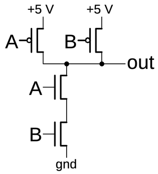
In a CMOS circuit, the NMOS and PMOS transistors work together, with the NMOS transistors pulling the output low as needed while the PMOS transistors pull the output high. By arranging the transistors in different ways, different logic gates can be created. The diagram below shows a NAND gate constructed from two PMOS transistors (top) and two NMOS transistors (bottom). If both inputs are high, the NMOS transistors turn on and pull the output low. But if either input is low, a PMOS transistor will pull the output high. Thus, the circuit below implements a NAND gate.
Notice that NMOS and PMOS transistors have an inherent inversion: a high input produces a low (for NMOS) or a low input produces a high (for PMOS). Thus, it is straightforward to produce logic circuits such as an inverter, NAND gate, NOR gate, or an AND-OR-INVERT gate. However, producing an XOR (exclusive-or) gate doesn't work with this approach: an XOR gate produces a 1 if either input is high, but not both.1 The XNOR (exclusive-NOR) gate, the complement of XOR, also has this problem. As a result, chips often have creative implementations of XOR gates.
The standard-cell two-gate XOR circuit
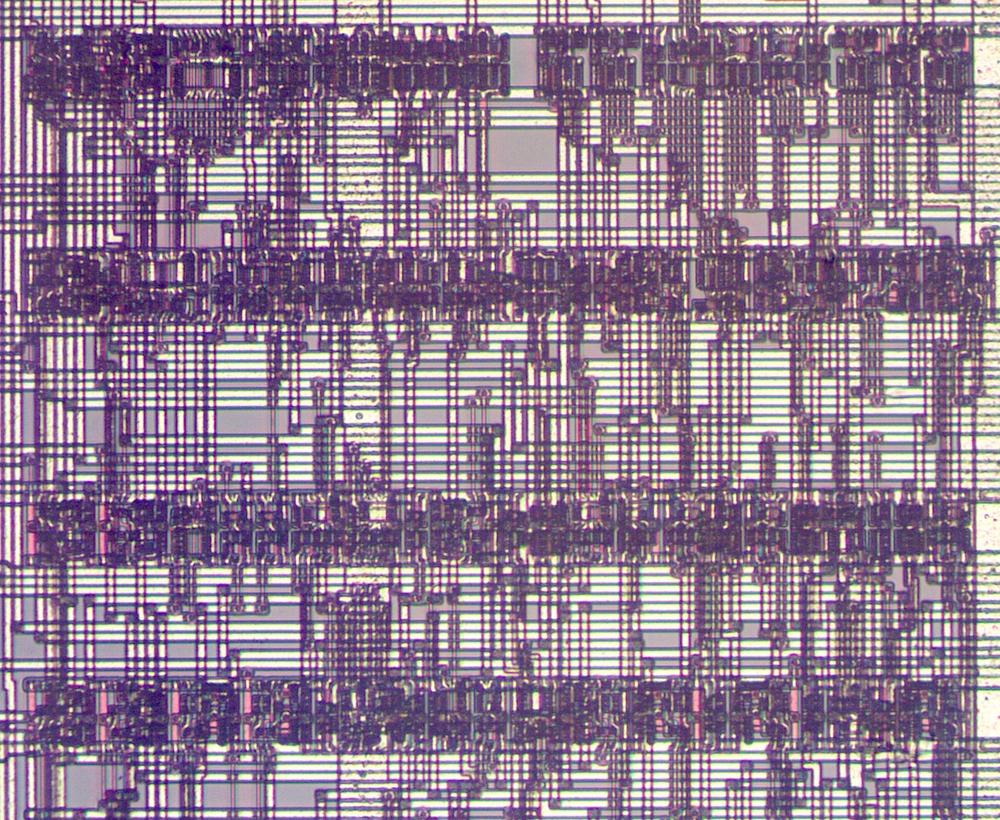
Parts of the 386 were implemented with standard-cell logic. The idea of standard-cell logic is to build circuitry out of standardized building blocks that can be wired by a computer program. In earlier processors such as the 8086, each transistor was carefully positioned by hand to create a chip layout that was as dense as possible. This was a tedious, error-prone process since the transistors were fit together like puzzle pieces. Standard-cell logic is more like building with LEGO. Each gate is implemented as a standardized block and the blocks are arranged in rows, as shown below. The space between the rows holds the wiring that connects the blocks.
The advantage of standard-cell logic is that it is much faster to create a design since the process can be automated. The engineer described the circuit in terms of the logic gates and their connections. A computer algorithm placed the blocks so related blocks are near each other. An algorithm then routed the circuit, creating the wiring between the blocks. These "place and route" algorithms are challenging since it is an extremely difficult optimization problem, determining the best locations for the blocks and how to pack the wiring as densely as possible. At the time, the algorithm took a day on a powerful IBM mainframe to compute the layout. Nonetheless, the automated process was much faster than manual layout, cutting weeks off the development time for the 386. The downside is that the automated layout is less dense than manually optimized layout, with a lot more wasted space. (As you can see in the photo above, the density is low in the wiring channels.) For this reason, the 386 used manual layout for circuits where a dense layout was important, such as the datapath.
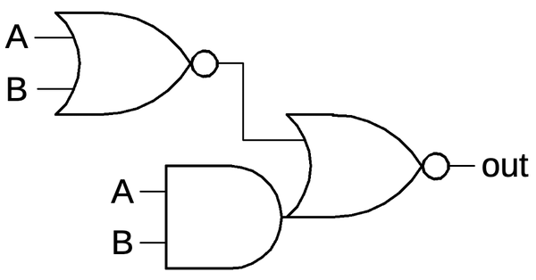
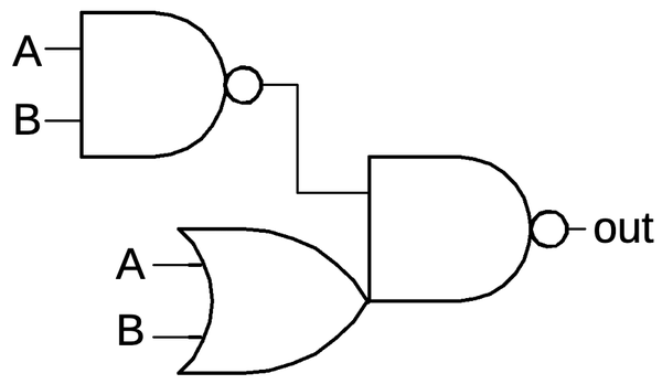
In the 386, the standard-cell XOR gate is built by combining a NOR gate with an AND-NOR gate as shown below.2 (Although AND-NOR looks complicated, it is implemented as a single gate in CMOS.) You can verify that if both inputs are 0, the NOR gate forces the output low, while if both inputs are 1, the AND gate forces the output low, providing the XOR functionality.
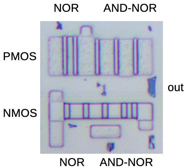
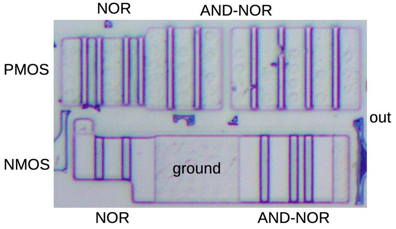
The photo below shows the layout of this XOR gate as a standard cell. I have removed the metal and polysilicon layers to show the underlying silicon. The outlined regions are the active silicon, with PMOS above and NMOS below. The stripes are the transistor gates, normally covered by polysilicon wires. Notice that neighboring transistors are connected by shared silicon; there is no demarcation between the source of one transistor and the drain of the next.
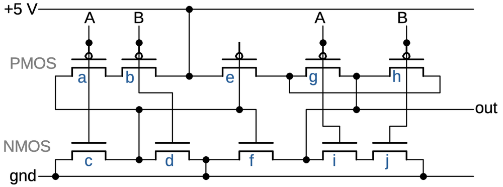
The schematic below corresponds to the silicon above. Transistors a, b, c, and d implement the first NOR gate. Transistors g, h, i, and j implement the AND part of the AND-NOR gate. Transistors e and f implement the NOR input of the AND-NOR gate, fed from the first NOR gate. The standard cell library is designed so all the cells are the same height with a power rail at the top and a ground rail at the bottom. This allows the cells to "snap together" in rows. The wiring inside the cell is implemented in polysilicon and the lower metal layer (M1), while the wiring between cells uses the upper metal layer (M2) for vertical connections and lower metal (M1) for horizontal connections. This strategy allows vertical wires to pass over the cells without interfering with the cell's wiring.
One important factor in a chip such as the 386 is optimizing the sizes of transistors. If a transistor is too small, it will take too much time to switch its output line, reducing performance. But if a transistor is too large, it will waste power as well as slowing down the circuit that is driving it. Thus, the standard-cell library for the 386 includes several XOR gates of various sizes. The diagram below shows a considerably larger XOR standard cell. The cell is the same height as the previous XOR (as required by the standard cell layout), but it is much wider and the transistors inside the cell are taller. Moreover, the PMOS side uses pairs of transistors to double the current capacity. (NMOS has better performance than PMOS so doesn't require doubling of the transistors.) Thus, there are 10 PMOS transistors and 5 NMOS transistors in this XOR cell.
The pass transistor circuit
Some parts of the 386 implement XOR gates completely differently, using pass transistor logic. The idea of pass transistor logic is to use transistors as switches that pass inputs through to the output, rather than using transistors as switches to pull the output high or low. The pass transistor XOR circuit uses 8 transistors, compared with 10 for the previous circuit.3
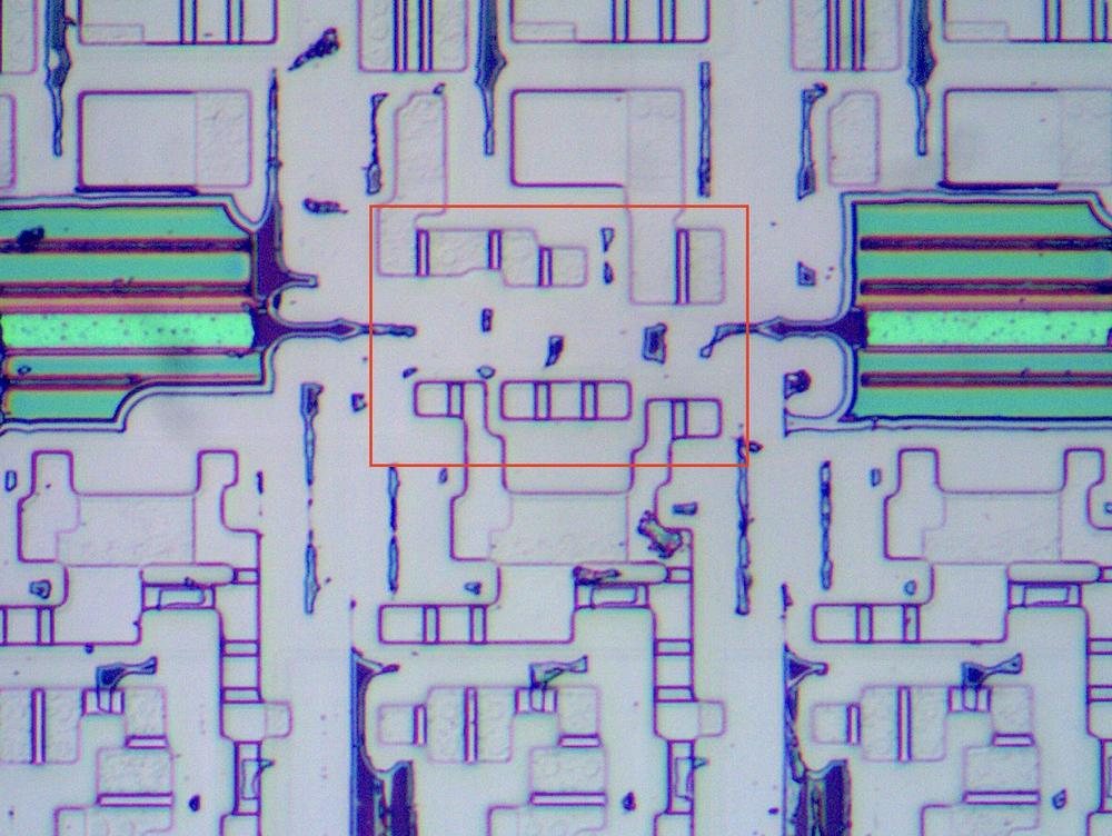
The die photo below shows a pass-transistor XOR circuit, highlighted in red. Note that the surrounding circuitry is irregular and much more tightly packed than the standard-cell circuitry. This circuit was laid out manually producing an optimized layout compared to standard cells. It has four PMOS transistors at the top and four NMOS transistors at the bottom.
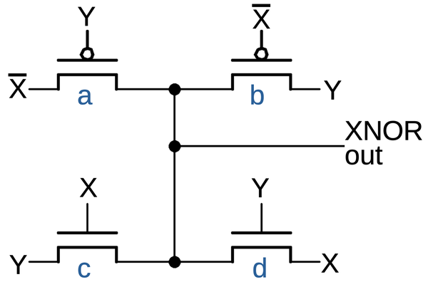
The schematic below shows the heart of the circuit, computing the exclusive-NOR (XNOR) of X and Y with four pass transistors. To understand the circuit, consider the four input cases for X and Y. If X and Y are both 0, PMOS transistor a will turn on (because Y is low), passing 1 to the XNOR output. (X is the complemented value of the X input.) If X and Y are both 1, PMOS transistor b will turn on (because X is low), passing 1. If X and Y are 1 and 0 respectively, NMOS transistor c will turn on (because X is high), passing 0. If X and Y are 0 and 1 respectively, transistor d will turn on (because Y is high), passing 0. Thus, the four transistors implement the XNOR function, with a 1 output if both inputs are the same.
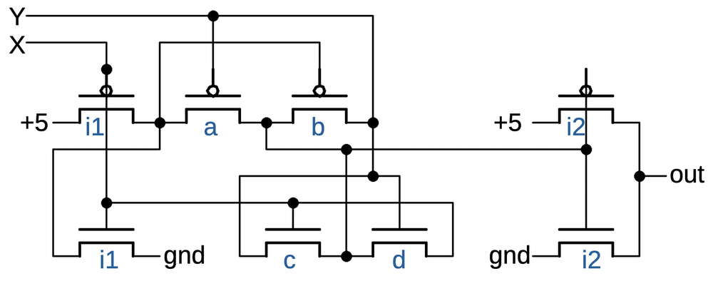
To make an XOR gate out of this requires two additional inverters. The first inverter produces X from X. The second inverter generates the XOR output by inverting the XNOR output. The output inverter also has the important function of buffering the output since the pass transistor output is weaker than the inputs. Since each inverter takes two transistors, the complete XOR circuit uses 8 transistors. The schematic below shows the full circuit. The i1 transistors implement the input inverter and the i2 transistors implement the output inverter. The layout of this schematic matches the earlier die photo.5
Conclusions
An XOR gate may seem like a trivial circuit, but there is more going on than you might expect. I think it is interesting that there isn't a single solution for implementing XOR; even inside a single chip, multiple approaches can be used. (If you're interested in XOR circuits, I also looked at the XOR circuit in the Z80.) It's also reassuring to see that even for a complex chip such as the 386, the circuitry can be broken down into logic gates and then understood at the transistor level.
I plan to write more about the 386, so follow me on Twitter @kenshirriff or RSS for updates. I'm also on Mastodon occasionally as @[email protected].
Notes and references
-
You can't create an AND or OR gate directly from CMOS either, but this isn't usually a problem. One approach is to create a NAND (or NOR) gate and then follow it with an inverter, but this requires an "extra" inverter. However, the inverter can often be eliminated by flipping the action of the next gate (using De Morgan's laws). For example, if you have AND gates feeding into an OR gate, you can change the circuit to use NAND gates feeding into a NAND gate, eliminating the inverters. Unfortunately, flipping the logic levels doesn't help with XOR gates, since XNOR is just as hard to produce. ↩
-
The 386 also uses XNOR standard-cell gates. These are implemented with the "opposite" circuit from XOR, swapping the AND and OR gates:
Schematic of an XNOR circuit. -
I'm not sure why some circuits in the 386 use standard logic for XOR while other circuits use pass transistor logic. I suspect that the standard XOR is used when the XOR gate is part of a standard-cell logic circuit, while the pass transistor XOR is used in hand-optimized circuits. There may also be performance advantages to one over the other. ↩
-
The first inverter can be omitted in the pass transistor XOR circuit if the inverted input happens to be available. In particular, if multiple XOR gates use the same input, one inverter can provide the inverted input to all of them, reducing the per-gate transistor count. ↩
-
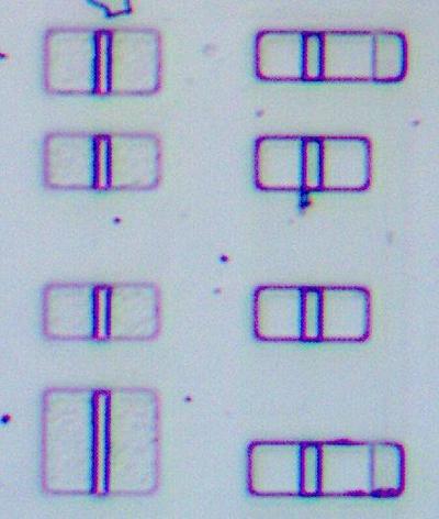
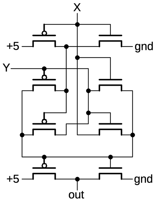
The pass transistor XOR circuit uses different layouts in different parts of the 386, probably because hand layout allows it to be optimized. For instance, the instruction decoder uses the XOR circuit below. This circuit has four PMOS transistors on the left and four NMOS transistors on the right.
An XOR circuit from the instruction decoder.The schematic shows the wiring of this circuit. Although the circuit is electrically the same as the previous pass-transistor circuit, the layout is different. In the previous circuit, several of the transistors were connected through their silicon, while this circuit has all the transistors separated and arranged in columns.
Schematic of the XOR circuit from the instruction decoder.
10 comments:
Fascinating article, as always. Thanks for continuing to do this research.
In the paragraph preceding the schematic of the XOR circuit, I believe "built by combining a NAND gate with an AND-NOR gate" should read "built by combining a NOR gate with an AND-NOR gate."
~~ Paul
Thanks, Paul. I've fixed that.
Is there any chance that the shift register passed the output of one XOR into the X input of another? If so, one of the inverters could be skipped, reducing the number of transistors and potentially speeding up the hot path as well.
Thanks for this addition to the Great CMOS XOR Zoo !
There are already many variations at
https://hackaday.io/project/8449-hackaday-ttlers/log/150147-bipolar-xor-gate-with-only-2-transistors
and now I have to add new topologies :-)
Yasep: wow, that is quite a collection of XOR circuits!
Ken : yes, indeed, and you contributed one with your analysis of the Z80 :-)
Why are XOR gates so ubiquitous?
Is it because XOR gates are essentially modulo 2?
A XOR gate basically provides a switchable inverter (one line controls if the signal on the other line gets inverted or not) which is very useful in many cases.
Additinally, every adder circuit and counter has xor circuits in it and they are very common in a cpu.
The XNOR implementation with four pass transistors has another interesting peculiarity. When X is 1, transistors b and c form a pass gate that connects the Y input to the output, which is also driven by one of transistors a (from inverted X) or d (from the X input). So if you want to change Y, whatever drives it needs to overcome those transistors briefly (until a and/or d change state), a little like an unbuffered Schmitt trigger. This requires strong drive for the inputs, or weak transistors in the gate. In the X=1, Y=1 case, transistor d also affects the X input to an extent. This would not fly as a general-purpose XOR gate.
Post a Comment