The Yamaha DX7 digital synthesizer (1983) was the classic synthesizer in 1980s pop music. It uses a technique called FM synthesis to produce complex, harmonically-rich sounds. In this blog post, I look inside its custom "OPS" sound chip and explain the control registers for this chip. By reverse-engineering the circuitry, I found a few undocumented test functions. (This post covers some fairly obscure details of the DX7; you might prefer my previous DX7 posts1 starting with "DX7 reverse-engineering".)
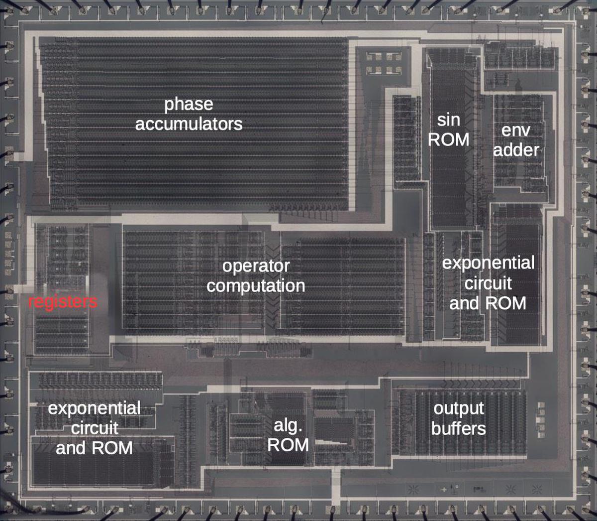
The die photo above shows the DX7's OPS sound synthesis chip under the microscope, showing its complex silicon circuitry. Unlike modern chips, this chip has just one layer of metal, visible as the whitish lines on top. Around the edges, you can see the 64 bond wires attached to pads; these connect the silicon die to the chip's 64 pins. In this blog post, I'm focusing on the control registers, highlighted in red. I'll outline the other functional blocks briefly. Each of the 96 oscillators has a phase accumulator used to generate the frequency. The sine and exponential functions are implemented with lookup tables in ROMs. Other functional blocks apply the envelope, hold configuration data, and buffer the output values.
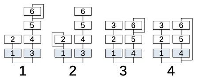
The DX7 generates sounds digitally using a technique called FM synthesis. Each note has six oscillators (called "operators") that can be combined in different ways (called "algorithms"). An algorithm is represented by a diagram (below), where an oscillator modulates the oscillator below, as shown by the lines. For instance, in algorithm 1 below, oscillator 6 modulates oscillator 5 which modulates 4 which modulates 3. Oscillator 2 modulates oscillator 1. The output is taken from the bottom oscillators (1 and 3). Meanwhile, oscillator 6 modulates itself, controlled by a user-selectable feedback level. With 32 different algorithms, the DX7 can generate a wide variety of sounds. In the DX7 synthesizer, all 16 notes must use the same algorithm. But from my reverse-engineering, it appears that the chip supports different algorithms for each note, even though the synthesizer doesn't make use of this.
To the programmer of the DX7 firmware, the sound chip appears to have two write-only registers that control the chip. The diagram below shows the layout of the chip's s two registers, as described by Anthony Richardson. The desired algorithm and feedback are written to address 1.2 Address 0 has bits to turn the "key sync" feature3 on and off. As for the Mute and Test Register Select bits, my investigation provides some explanation.
Address | Bit 7 | Bit 6          | Bit 5        | Bit 4 | Bit 3 | Bit 2 | Bit 1 | Bit 0 |
0       | Mute  | Clear Key Sync | Set Key Sync | Test Register Select                  |
1       | Algorithm Select (0..31)                              | Feedback Level (0..7) |
(The functionality above is pretty limited, so you might wonder how the synthesizer controls which notes are played. Most of the synthesizer functions are controlled through a second custom chip, the envelope generator chip (EGS). Note and envelope data is written to registers in the EGS chip, which then sends frequency and amplitude data to the sound chip over a special bus.)
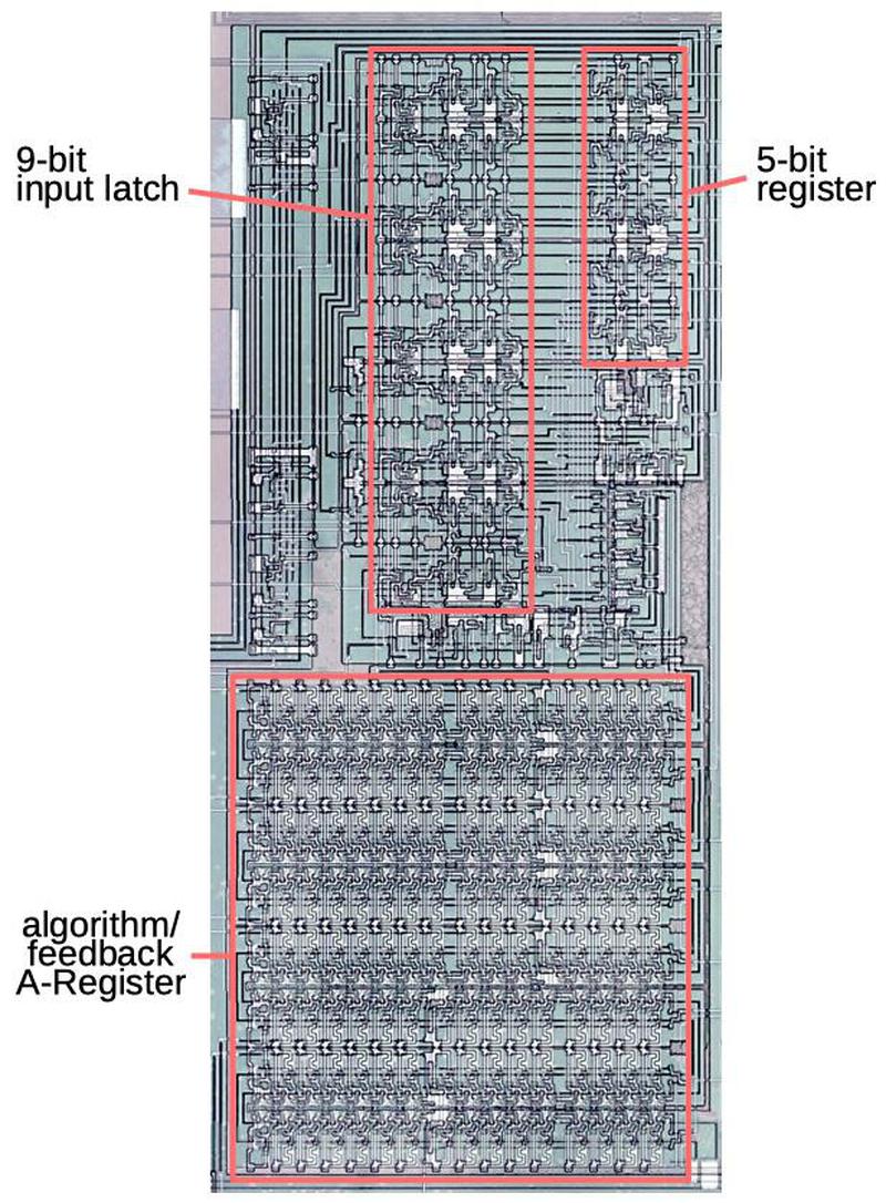
The diagram below shows the main components of the register circuitry. The large block at the bottom is the A-register, which holds the algorithm/feedback entries, as 16 8-bit values.4 The most puzzling feature of the A-register is its size; it holds 16 entries, one for each note, but the DX7 uses the same algorithm/feedback setting for all 16 notes. The second puzzling feature is that although the chip appears to have two 8-bit registers, the implementation is one 9-bit register, and one 5-bit register. Moreover, the 5-bit register can only be modified by writing through the 9-bit register.
The chip has one address pin (called "DS") which selects between the two registers. When a byte is written to the chip, to either address, the 8 bits along with DS (the address bit) are stored in the 9-bit latches. If DS is 0 (i.e. write to the control address 0), the bits are decoded to perform any special functions, and the lower 5 bits are loaded into the 5-bit register on the right. If DS is 1 (i.e. write to the algorithm/feedback address 1), the 8-bit algorithm/feedback value is stored into the A register, in a location controlled by the 5-bit register.
Updating the algorithm/feedback
The algorithm/feedback A-register register holds data for 16 notes. It can be updated in two ways. The first way, used by the DX7, updates all entries with the same value. The second way updates a single entry, allowing different notes to have different algorithms. Both cases involve a write to address 0, followed by writing the algorithm/feedback byte to address 1.
To update all entries, address 0 must be written with a value with the bit pattern 0??1?0?? (where ? indicates a "don't care" bit that can be 0 or 1).5
This pattern triggers a circuit that constantly loads the value in the data latch into the storage register.
The DX7's CPU controls the OPS chip in this way. Specifically, an update of the algorithm and feedback is performed by writing either 0x30 (if sync is on) or 0x50 (if sync is off) to address 0, and then writing the algorithm/feedback byte to address 1.2
The second update path will change the algorithm and feedback for a single note.
(The DX7 does not use this feature.)
is triggered by writing the bit pattern 0??0nnnn, where nnnn specifies one of the 16 notes.
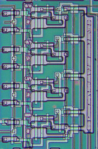
The implementation of this is a bit tricky because the chip uses shift registers for storage, not RAM. The A-register consists of 8 shift registers (one for each bit), each with 16 stages (one for each note). An entry can only be updated when it is shifted out the end of the shift register, and a new value can be inserted. (This is unlike RAM, where an arbitrary entry can be written.) To update an entry in the shift register, a 4-bit comparator circuit (below) compares the number of the current note with the number of the desired note in the control register. When there is a match, the new value is written to the shift register.
Special command sequences
The logic circuitry recognizes several bit patterns when they are written to address 0, and causes special actions when they are detected. These are not used by the DX7; I think they were used for testing the chip during manufacturing to make tests more predictable and faster.
1???????: Setting the top bit triggers several special actions. Earlier analysis has labeled this bit as "Mute", but I suspect
it is more of a "Test Reset" function,
resetting the chip to a known state so tests will be predictable.
This bit clears the phase accumulators.
This bit disables the scale factors, so the output data is unshifted.
It also bypasses the output latch, which may output digital note data at a higher rate.
1??????1: In addition to the previous action, this pattern resets the counters that count through the operators and notes,
controlling the actions of the chip.
This is probably used start testing the chip from a known state, so the outputs can be compared with expected values.
1?????1?: This causes the low-order bits of the phase register to generate the waveform, rather than the high-order bits.
I think this is used for testing so the low-order bits can be examined more directly to find flaws.
It also will increase the frequencies by a factor of 1024, which may help run through waveforms faster for testing.
Conclusion
By looking inside the chip and reverse-engineering the silicon circuits, I learned some details about the internal registers. One interesting discovery is that the chip appears to support separate algorithms for each voice, even though the synthesizer doesn't use this feature. I also uncovered some test functionality.
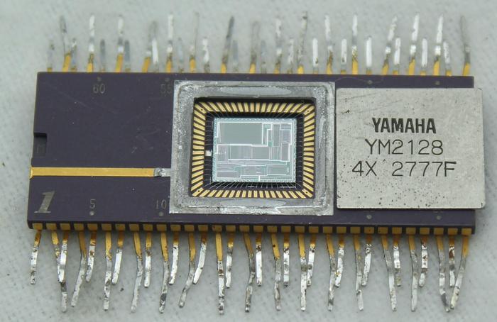
I plan to continue investigating the DX7's circuitry, so follow me on Twitter @kenshirriff for updates. I also have an RSS feed. Thanks to Jacques Mattheij and Anthony Richardson for providing the chip and discussion.6
Disclaimer: I figured out the behavior described in this post studying the die. It hasn't been tested on an actual DX7 so I don't guarantee that it is correct.
Notes and references
-
My previous posts on the DX7: DX7 reverse-engineering, The exponential ROM, The log-sine ROM, How algorithms are implemented, and The output circuitry. ↩
-
Looking at the ROM shows how the synthesizer's CPU communicates with the OPS chip. Since the DX7 ROM code has been disassembled, you can view the code that writes to the sound chip here. ↩↩
-
Oscillator Key Sync is a feature of the DX7. According to the manual, Operator Key Sync "enables you to set the operator so its 'oscillator' begins at the start of the sine wave cycle each time you play a note. When Oscillator Key Sync is off, the sine wave continues so that subtle differences will occur even when you play the note repeatedly." ↩
-
The DX7/9 Service Manual shows the "A-register" holding the algorithm and feedback level, so I'll use that name. ↩
-
The bit pattern
0??1?0??looks a bit random. I don't know why this pattern was chosen. The first two bits can be explained, but I don't see a purpose for the last 0 bit. ↩ -
For more information on the DX7 internals, see DX7 Technical Analysis, DX7 Hardware, OPLx decapsulated, and the video Emulating the DX7 the hard way. ↩

1 comment:
Sorry if I missed in all the posts... but did you figure out what the mystery ROM was all about? Thanks!
Post a Comment