How it works
The iPhone power adapter is a switching power supply, where the input power is switched on and off about 70,000 times a second in order to get the exact output voltage required. Because of their design, switching power supplies are generally compact and efficient and generate little waste heat compared to simpler linear power supplies.In more detail, the AC line power is first converted to high voltage DC[1] by a diode bridge. The DC is switched on and off by a transistor controlled by a power supply controller IC. The chopped DC is fed into a flyback[2] transformer which converts it into low voltage AC. Finally, this AC is converted into DC which is filtered to obtain smooth power free of interference, and this power is output through the USB jack. A feedback circuit measures the output voltage and sends a signal to the controller IC, which adjusts the switching frequency to obtain the desired voltage.
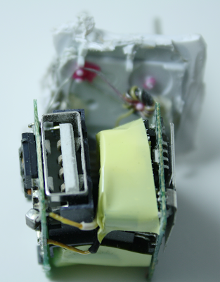
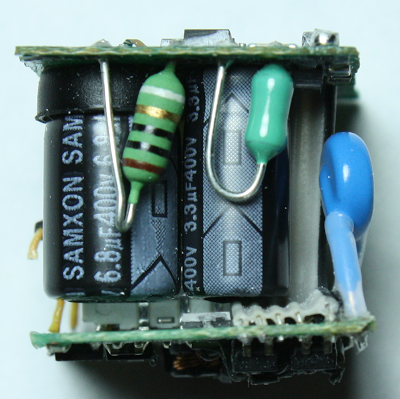
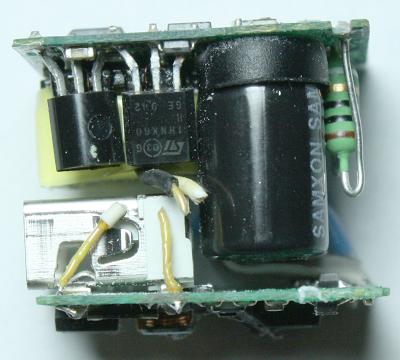
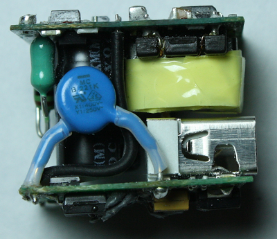
The side view above shows some of the larger components. The charger consists of two circuit boards, slightly under one inch square each.[3] The top board is the primary, which has the high voltage circuitry, and the bottom board, the secondary, has the low voltage output circuitry. The input AC first passes through a fusible resistor (striped), which will break the circuit if there is a catastrophic overload. The input AC is converted to high-voltage DC, which is smoothed by the two large electrolytic capacitors (black with white text and stripe) and the inductor (green).
Next, the high voltage DC is chopped at high frequency by a MOSFET switching transistor, which is the large three-pinned component in the upper left. (The second transistor clamps voltage spikes, as will be explained below.) The chopped DC goes to the flyback transformer (yellow, barely visible behind the transistors), which has low voltage output wires going to the secondary board below. (These wires were cut during disassembly.) The secondary board converts the low voltage from the transformer to DC, filters it, and then feeds it out through the USB connector (the silver rectangle in the lower left). The gray ribbon cable (just barely visible on the lower right under the capacitor) provides feedback from the secondary board to the controller IC to keep the voltage regulated.
The picture above shows the flyback transformer (yellow) more clearly, above the USB jack. The large blue component is a special "Y" capacitor[4] to reduce interference. The controller IC is visible above the transformer on the top of the primary board.[5]
The circuit in detail
The primary
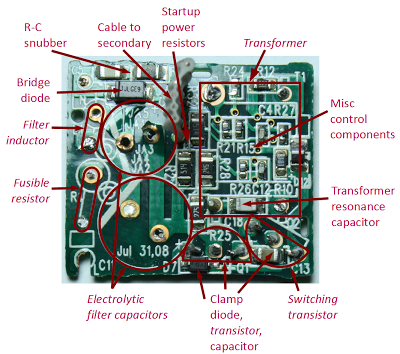
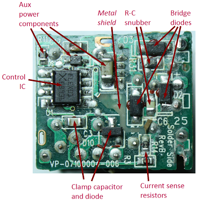
The primary circuit board is packed with surface mounted components on both sides. The inner side (diagram above) holds the large components while the outer side (diagram below) has the controller IC. (The large components were removed in the diagrams, and are indicated in italics.) Input power is connected to the corners of the board, goes through the 10Ω fusible resistor, and is rectified to DC by the four diodes. Two R-C snubber circuits absorb EMI interference created by the bridge.[6] The DC is filtered by the two large electrolytic capacitors and the inductor, producing 125-340V DC. Note the thickness of the circuit board traces connecting these capacitors and other high-current components compared to the thin control traces.
The power supply is controlled by an 8-pin STMicrosystems L6565 quasi-resonant SMPS controller chip.[7] The controller IC drives the MOSFET switching transistor which chops the high voltage DC and feeds it into the primary winding of the flyback transformer. The controller IC takes a variety of inputs (secondary voltage feedback, input DC voltage, transformer primary current, and transformer demagnetization sensing) and adjusts the switching frequency and timing to control the output voltage through complex internal circuitry. The current sense resistors let the IC know how much current is flowing through the primary, which controls when the transistor should be turned off.
The second switching transistor, along with some capacitors and diodes, is part of a resonant clamp circuit that absorbs voltage spikes on the transformer. This unusual and innovative circuit is patented by Flextronics.[8][9]
The controller IC needs DC power to run; this is provided by an auxiliary power circuit consisting of a separate auxiliary winding on the transformer, a diode, and filter capacitors. Since the controller IC needs to be powered up before the transformer can start generating power, you might wonder how this chicken-and-egg problem gets solved. The solution is the high-voltage DC is dropped to a low level through startup power resistors to provide the initial power to the IC until the transformer starts up. The auxiliary winding is also used by the IC to sense transformer demagnitization, which indicates when to turn on the switching transistor.[7]
The secondary
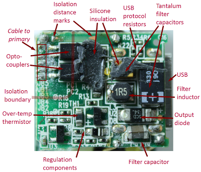
On the secondary board, the low voltage AC from the transformer is rectified by the high-speed Schottky diode, filtered by the inductor and capacitors, and connected to the USB output. The tantalum filter capacitors provide high capacitance in a small package.The USB output also has specific resistances connected to the data pins to indicate to the iPhone how much current the charger can supply, through a proprietary Apple protocol.[10] An iPhone displays the message "Charging is not supported with this accessory" if the charger has the wrong resistances here.
The secondary board contains a standard switching power supply feedback circuit that monitors the output voltage with a TL431 regulator and provides feedback to the controller IC through the optocoupler. A second feedback circuit shuts down the charger for protection if the charger overheats or the output voltage is too high.[11] A ribbon cable provides this feedback to the primary board.
Isolation
Because the power supply can have up to 340V DC internally, safety is an important issue. Strict regulations govern the separation between the dangerous line voltage and the safe output voltage, which are isolated by a combination of distance (called creepage and clearance), and insulation. The standards[12] are somewhat incomprehensible, but roughly 4mm of distance is required between the two circuits. (As I discuss in Tiny, cheap, dangerous: Inside a (fake) iPhone charger, cheap chargers totally ignore these safety rules.)You might expect the primary board to have the dangerous voltages and the secondary board to have the safe voltages, but the secondary board consists of two areas: the hazardous area connected to the primary board, and the low-voltage area. The isolation boundary between these areas is about 6mm in the Apple charger and can be seen in the above diagram. This isolation boundary ensures that dangerous voltages cannot reach the output.
There are three types of components that cross the isolation boundary, and they must be specially designed for safety. The key component is the transformer, which provides a way for electrical power to reach the output without a direct electrical connection. Internally, the transformer is extensively insulated, as will be shown below. The second component type is the optocouplers, which send the feedback signal from the secondary to the primary. Internally, the optocoupler contains a LED and a photo-transistor, so the two sides are connected only by light, not by an electrical circuit. (Note the silicone insulation on the secondary side of the optocouplers to provide extra safety.) Finally, the Y capacitor is a special type of capacitor[4] that lets EMI (electromagnetic interference) escape between the high-voltage primary and the low-voltage secondary.
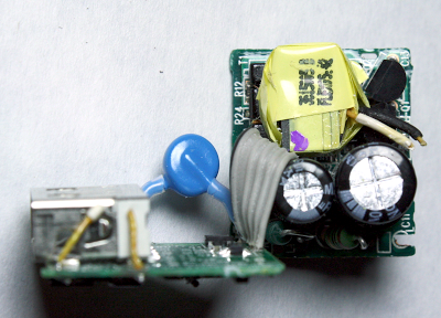
The above picture shows some of the isolation techniques. The secondary board (left) has the blue Y capacitor. Note the lack of components in the middle of the secondary board, forming an isolation boundary. The components on the right of the secondary board are connected to the primary board by the gray ribbon cable so they are at potentially high voltages. The other connection between the boards is the pair of wires from the flyback transformer (yellow) delivering the output power to the secondary board; these were cut to separate the boards.
Schematic
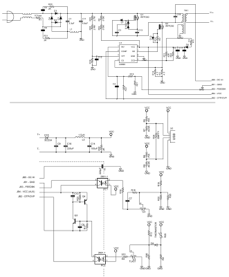
I've put together an approximate schematic showing the charger circuit.[13] Click for a larger version.These circuits are very small
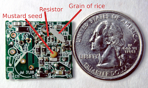
Looking at these pictures, it's easy to lose track of how very small these components are, and how the charger crams all this complexity into one inch. The following slightly magnified picture shows a quarter, a grain of rice, and a mustard seed to give a size comparison. Most of the components are surface-mount devices which are soldered directly to the printed circuit board. The smallest components, such as the resistor pointed out in the picture, are known as "0402" size since they are .04 inches by .02 inches. The larger resistors to the left of the mustard seed handle more power and are known as "0805" size since they are .08 x .05 inches.Transformer teardown
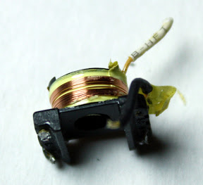
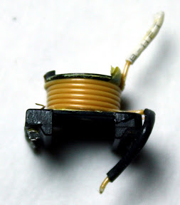
The flyback transformer is the key component of the charger, the largest component, and probably the most expensive.[14] But what's inside? I took apart the transformer to find out.The transformer measures roughly 1/2" by 1/2" by 1/3". Inside, the transformer has three windings: a high voltage primary input winding, a low voltage auxiliary winding to provide power to the control circuits, and a high-current low voltage output winding. The output winding is connected to the black and white wires coming out of the transformer, while the other windings are connected to the pins attached to the bottom of the transformer.
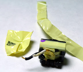
The outside of the transformer has a couple layers of insulating tape. The second line appears to start with "FLEX", for Flextronics. Two grounded strands of wire are wrapped around the outside of the transformer to provide shielding.
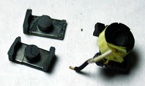
After removing the shielding and the tape, the two halves of the ferrite core can be removed from the windings. Ferrite is a rather brittle ceramic material, so the core broke during removal. The core surrounds the windings and contains the magnetic fields. Each core piece is roughly 6mm x 11mm x 4mm; this style of core is known as EQ. The circular center section is very slightly shorter than the ends, creating a small air gap when the core pieces are put together. This 0.28mm air gap stores the magnetic energy for the flyback transformer.
Underneath the next two layers of tape is a 17-turn winding of thin varnished wire, which I think is another shield winding to return stray interference to ground.
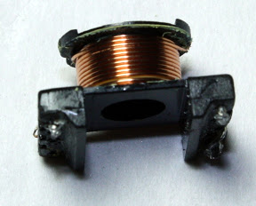
Underneath the shield and another two layers of tape is the 6-turn secondary output winding that is connected to the black and white wires. Note that this winding is heavy-gauge wire, since it is feeding the 1A output. Also note that the winding is triple-insulated, which is a UL safety requirement to ensure that the high voltage primary remains isolated from the output. This is one place where cheap chargers cheat - they just use regular wire instead of triple-insulated, and also skimp on the tape. The result is there's not much protecting you from high voltage if there's an insulation flaw or power surge.
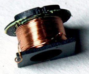
Under the next double layer of tape is the 11-turn heavy gauge primary power winding, that powers the controller IC. Since this winding is on the primary side, it doesn't need to be triple insulated. It's just insulated with a thin layer of varnish.
Under the final double layer of tape is the primary input winding, which is 4 layers of approximately 23 turns each. This winding receives the high voltage input. Since the current is very low, the wire can be very thin. Because the primary has about 15 times as many turns as the secondary winding, the secondary voltage will be 1/15 the primary voltage, but 15 times the current. Thus, the transformer converts the high voltage input to low voltage, high current output.
The final picture shows all the components of the transformer; left to right shows the layers from the outside tape to the innermost winding and bobbin.
Apple's huge profit margins
I was surprised to realize how enormous Apple's profit margins must be on these chargers. These chargers sell for about $30Apple's 2008 charger safety recall
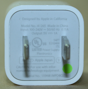
In 2008, Apple recalled the iPhone chargers due to a defect that the AC prongs could fall off the charger and get stuck in an outlet.[15] The faulty chargers had the prongs attached with what was described as little more than glue and "wishful thinking".[15] Apple replaced the chargers with a redesigned model indicated by the green dot marking shown above (which counterfeit chargers inevitably imitate).
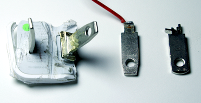
I decided to see what safety improvements Apple made in the replacement charger, and compare with other similar chargers. I tried pulling out the prongs of the Apple charger, a Samsung charger, and a counterfeit charger. The counterfeit prongs came out with a tug with pliers, as there's basically nothing anchoring them but friction. The Samsung prongs took a lot of pulling and twisting with pliers, since they have little metal tabs holding them in place, but eventually they came out.
When I moved on to the Apple charger, the prongs didn't budge, even with my hardest pulling with pliers, so I got out the Dremel and ground through the case to find out what was holding the prongs. They have large metal flanges embedded in the plastic of the case, so there's no way a prong can come loose short of the destruction of the charger. The photo shows the Apple plug (note the thickness of plastic removed from the right half), the prong from the counterfeit charger held in only by friction, and the Samsung prong held in by small but sturdy metal tabs.
I'm impressed with the effort Apple put into making the charger more safe after the recall. They didn't just improve the prongs slightly to make them more secure; clearly someone was told to do whatever it takes to make sure there's absolutely no way the prongs could possibly come loose again under any circumstances.
What makes Apple's iPhone charger special
Apple's power adapter is clearly a high-quality power supply designed to produce carefully filtered power. Apple has obviously gone to extra effort to reduce EMI interference, probably to keep the charger from interfering with the touchscreen.[16] When I opened the charger up, I expected to find a standard design, but I've compared the charger to the Samsung charger and several other high-quality industry designs,[17] and Apple goes beyond these designs in several ways.The input AC is filtered thorugh a tiny ferrite ring on the plastic case (see photo below). The diode bridge output is filtered by two large capacitors and an inductor. Two other R-C snubbers filter the diode bridge, which I've only seen elsewhere in audio power supplies to prevent 60Hz hum;[6] perhaps this enhances the iTunes listening experience. Other chargers I disassembled don't use a ferrite ring and usually only a single filter capacitor. The primary circuit board has a grounded metal shield over the high-frequency components (see photo), which I haven't seen elsewhere. The transformer includes a shield winding to absorb EMI. The output circuit uses three capacitors including two relatively expensive tantalum ones[14] and an inductor for filtering, when many supplies just use one capacitor. The Y capacitor is usually omitted from other designs. The resonant clamp circuit is highly innovative.[9]
Apple's design provides extra safety in a few ways that were discussed earlier: the super-strong AC prongs, and the complex over-temperature / over-voltage shutdown circuit. Apple's isolation distance between primary and secondary appears to go beyond the regulations.
Conclusions
Apple's iPhone charger crams a lot of technology into a small space. Apple went to extra effort to provide higher quality and safety than other name-brand chargers, but this quality comes at a high cost.If you're interested in power supplies, please take a look at my other articles: tiny, cheap, dangerous: Inside a (fake) iPhone charger, where I disassemble a $2.79 iPhone charger and discover that it violates many safety rules; don't buy one of these. Also take a look at Apple didn't revolutionize power supplies; new transistors did which examines the history of switching power supplies. To see Apple's adapter disassembled, check out videos created by scourtheearth and Ladyada. Finally, if you have an interesting charger lying around that you don't want, send it to me and maybe I'll write up a detailed teardown of it.
Also see comments on Hacker News.
Notes and references
[1] You might wonder why the DC voltage inside the power supply is so much higher than the line voltage. The DC voltage is approximately sqrt(2) times the AC voltage, since the diode charges the capacitor to the peak of the AC signal. Thus, the input of 100 to 240 volts AC is converted to a DC voltage of 145 to 345 volts internally. This isn't enough to be officially high voltage but I'll call it high voltage for convenience. According to standards, anything under 50 volts AC or 120 V dc is considered extra-low voltage and is considered safe under normal conditions. But I'll refer to the 5V output as low voltage for convenience.[2] The Apple power supply uses a flyback design, where the transformer operates "backwards" from how you might expect. When a voltage pulse is sent into the transformer, the output diode blocks the output so there is no output - instead a magnetic field builds up. When the voltage input stops, the magnetic field collapses causing voltage output from the transformer. Flyback power supplies are very common for low-wattage power supplies.
[3] The primary board measures about 22.5mm by 20.0mm, while the secondary board is about 22.2mm by 20.2mm. [4] For more information on X and Y capacitors, see Kemet's presentation and Designing low leakage current power supplies.
[5] For clarity, some insulation was removed before taking the pictures in this article. The Y capacitor was covered with black heat shrink tubing, there was tape around the side of the circuit, the fusible resistor was covered with black heat shrink tubing, and there was a black insulating cover over the USB connector.
[6] Snubber circuits can be used to reduce 60 Hz hum generated by the diode bridge in audio power supplies. A detailed reference on R-C snubbers for audio power supply diodes is Calculating Optimum Snubbers, and a sample design is An Audio Amplifier Power Supply Design.
[7] The power supply is controlled by the L6565 quasi-resonant SMPS (switched-mode power supply) controller chip (datasheet). (To be sure, the chip could be something else, but the circuit exactly matches the L6565 and no other chip I examined.)
To improve efficiency and reduce interference, the chip uses a technique known as quasi-resonance, which was first developed in the 1980s. The output circuit is designed so when the power is switched off, the transformer voltage will oscillate. When the voltage hits zero, the transistor switches back on. This is known as Zero Voltage Switching because the transistor is switched when there is essentially no voltage across it, minimizing wasted power and interference during switching. The circuit remains on for a variable time (depending on the power required), and then switches back off, repeating the process. (See Exploring quasi-resonant converters for power supplies for more information.)
One interesting consequence of quasi-resonance is the switching frequency varies depending on the load (with 70kHz as a typical value). Early power supplies such as the Apple II power supply used simple variable-frequency circuits to regulate the power. But in the 1980s, these circuits were replaced by controller ICs that switched at a fixed frequency, but varied the width of the pulses (known as PWM). Now, advanced controller ICs have gone back to variable frequency controls. But in addition, super-cheap knockoff power supplies use variable frequency circuits almost identical to the Apple II. So both high-end and low-end chargers are now back to variable frequency.
It took me a long time to realize that the "FLEX01" marking on the controller IC indicates Flextronics, and the X on the chip was from the Flextronics logo:
![]() .
I assume the chip has these markings because it is being manufactured for Flextronics. The "EB936" marking on the chip could be Flextronics' own part number, or a date code.
.
I assume the chip has these markings because it is being manufactured for Flextronics. The "EB936" marking on the chip could be Flextronics' own part number, or a date code.
[8] I thought Flextronics was just an electronics assembler and I was surprised to learn that Flextronics does a lot of innovative development and has literally thousands of patents. I think Flextronics should get more credit for their designs. (Note that Flextronics is a different company than Foxconn, which manufactures iPads and iPhones and has the controversy over working conditions).
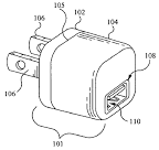
The picture above is from Flextronics Patent 7,978,489: Integrated Power Converters describes an adapter that looks just like the iPhone charger. The patent itself is a grab bag of 63 assorted claims (spring contacts, EMI shields, thermal potting material), most of which are not actually relevant to the iPhone charger.
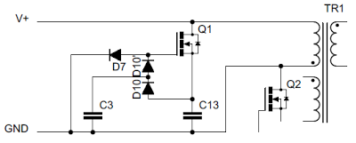
[9] Flextronics Patent 7,924,578: Two Terminals Quasi Resonant Tank Circuit describes the resonance circuit used in the iPhone charger, which is shown in the following diagram. Transistor Q2 drives the transformer. Transistor Q1 is the clamp transistor, which directs the voltage spike from the transformer into resonance capacitor C13. The innovative part of this circuit is that Q1 doesn't need special drive circuitry like other active clamp circuits; it is self-powered via the capacitors and diodes. Most charger power supplies, by contrast, use a simple resistor-capacitor-diode clamp which dissipates the energy in the resistor.[18]
Later Flextronics patents extend the resonance circuit with even more diodes and capacitors: see patents 7,830,676, 7,760,519, and 8,000,112
[10] Apple indicates the charger type through a proprietary technique of resistances on the USB D+ and D- pins. For details on USB charging protocols, see my earlier references.
[11] One puzzling feature of the Apple charger is the second feedback circuit monitoring the temperature and output voltage. This circuit on the secondary board consists of a thermistor, a second 431 regulator, and a few other components to monitor the temperature and voltage. The output is connected through a second optocoupler to more circuitry on other side of the secondary board. Two transistors are wired in a SCR-like crowbar latch that will short out the auxiliary power and also shut down the controller IC. This circuit seems excessively complex for this task, especially since many controller ICs have this functionality built in. I could be misunderstanding this circuit, because it seems that Apple unnecessarily took up space and expensive components (maybe 25 cents worth) implementing this feature in such a complex way.
[12] Note the mysterious "For use with information technology equipment" on the outside of the charger. This indicates that the charger is covered by the safety standard UL 60950-1, which specifies the various isolation distances required. For a brief overview of isolation distances, see i-Spec Circuit Separation and some of my earlier references.
[13] Some notes on the components used: On the primary board, the JS4 package is two diodes in a single package. The input diodes labeled 1JLGE9 are 1J 600V 1A diodes. The switching transistors are 1HNK60 600V 1A N-channel MOSFETs. The values of many of the resistors and capacitors are indicated through standard SMD three-digit markings (two digits and then a power of ten, giving ohms or picofarads).
On the secondary board, the "330 j90" capacitor is a Sanyo POSCAP tantalum polymer 300mF 6.3V capacitor (j indicates 6.3V and 90 is a date code). 1R5 indicates a 1.5uH inductor. GB9 is a AS431I low cathode current adjustable precision shunt regulator, and 431 is a regular TL431 regulator. SCD34 is a 3A 40V schottky rectifier. YCW is an unidentified NPN transistor and GYW is an unidentified PNP transistor. The Y capacitor labeled "MC B221K X1 400V Y1 250V" is a 220pF Y capacitor. The "107A" capacitor is a 100 µF 10V tantalum capacitor (A indicates 10V). The optocouplers are PS2801-1. (All these component identifications should be considered tentative, along with the schematic.)
[14] In order to get a rough idea of how much the components in the charger cost, I looked up the prices of some components on octopart.com. These prices are the best prices I could find after a brief search, in quantities of 1000, attempting to match the parts accurately. I have to assume Apple's prices are considerably better than these prices.
| Component | Price |
|---|---|
| 0402 SMD resistor | $0.002 |
| 0805 SMD capacitor | $0.007 |
| SMD transistor | $0.02 |
| fusible resistor | $0.03 |
| 1A 600V (1J) diode | $0.06 |
| thermistor | $0.07 |
| Y capacitor | $0.08 |
| 3.3uF 400V electrolytic capacitor | $0.10 |
| TL431 | $0.10 |
| 1.5uH inductor | $0.12 |
| SCD 34 diode | $0.13 |
| 2801 optocoupler | $0.16 |
| 1HNK60 transistor | $0.22 |
| USB jack | $0.33 |
| 100uF tantalum capacitor | $0.34 |
| L6565 IC | $0.55 |
| 330uF tantalum polymer capacitor (Sanyo POSCAP) | $0.98 |
| flyback transformer | $1.36 |
A few notes. Flyback transformers are generally custom and prices are all over the place, so I don't have much confidence in that price. I think the POSCAP price is high because I was looking for the exact manufacturer, but tantalum capacitors are fairly expensive in general. It's surprising how cheap SMD resistors and capacitors are: a fraction of a penny.
[15] Apple's safety recall of chargers was announced in 2008. Blog reports showed that the prongs on the charger were attached only by 1/8" of metal and some glue. Apple Recalls iPhone 3G Power Adapters in Wired provides more details.
[16] Low-quality chargers interfere with touchscreens, and this is described in detail in Noise Wars: Projected capacitance strikes back. (Customers also report touchscreen problems from cheap chargers on Amazon and other sites.)
[17] There are many industry designs for USB AC/DC converters in the 5W range. Sample designs are available from iWatt, Fairchild, STMicroelectronics, Texas Instruments, ON Semiconductor, and Maxim.
[18] When a diode or transistor switches, it creates a voltage spike, which can be controlled by a snubber or clamp circuit. For a lot of information on snubbers and clamps, see Passive Lossless Snubbers for High Frequency PWM Conversion and Switchmode Power Supply Reference Manual.
175 comments:
Fantastic read! Thanks for doing this. It's geeky stuff like this that makes the net so darn addicting.- I mean power supplies?? Who knew?
Is it possible that the higher quality IC helps this charger truly switch off when a device is not connected? I've read that this Apple's adapters have effectively no waste when not in use, unlike most that always use some energy when connected to the AC receptacle.
Matthew: surprisingly, it turns out that Apple's charger uses more power when not in use than the other chargers I measured (a Samsung charger and several $2 knockoff chargers). The idle power is still low - about 0.3 watts. I plan to write an article about power usage later.
A link to an Amazon product page! This has to be one of the best affiliate sales I've ever seen. Itwould actually make me feel better buying the charger. Nice writeup.
You say that the 30 bucks Apple charges for these chargers will be profit, mainly. Perhaps that is the case. Seeing how much thought went into these things, knowing a recall and a redesign happened, reading how the design goes above and beyond safety regulations, I dare assume Apple spent a lot of time on research, prototyping, and testing. That time is an expensive investment and I'd say a large part of the margin goes into returning that investment. At some point, obviously, that ROI will be met and the remaining sales will turn into profit... part of which indubidably will be invested again for the next gadget.
Excellent post!
I've been wondering why the presumably high-quality samsung charger that came with my Galaxy Nexus emits an ultra high pitched squeal (which wavers a bit) when plugged in, but that goes away when the phone's plugged in.
Based on your article I'm guessing it's the switching frequency, which you said is usually ~70kHz but varies depending on load, so maybe it dips into the top of the audible range when there's nothing plugged in? I'm still left wondering what's physically resonating to create the sound...
I believe the model on the charger is ETA0U80JBEBSTD.
Have you done a disassembly of the Kindle usb charger? It also has some Flextronics work. Would like to see the contrast with Apple’s specs. While Amazon has a smaller charger that can fit even more easily in a pocket, they were kind of notorious for having usb cables that disintegrated in under a year.
The physical vibrations come from the wiring of the inductor or transformer. Current moving through a wire creates a coupling force on the nearby wires pulling them closer and then pushing them away, when the current stops flowing at the end of the cycle. The wires displace a tiny amount on each oscillation of the drive waveform. Given that the coil has many hundred turns of wire, each of which, is displacing, the sound pressure generated by the movement can amount to something noticeable if it is in the audio band. This problem usually gets more noticeable as the power supply ages. Manufacturers coat the coil with glue to reduce the movement of the wires. As the component ages, the glue becomes more brittle and may crack or otherwise yield allowing the wires to displace more freely.
Great article. I am a super tough sell on that account, too. Extremely well done and technically accurate; a pleasure to read. I appreciate this level of engineering too, but seldom see anyone doing such a thorough job of exploring the details of it online. Thanks for the effort and the observations
So interesting! Thank you so much for this great article! I love reading about all of the little things!
Great article, thanks. One complaint, though, regarding your definition of "profit." I build scientific instruments for a living, and I assure you, the cost of parts is one of many, many costs that a builder has to recover in the selling price; for me, labor and other overhead dwarf parts on some products.
Except that they put shitty connectors that fray much quicker than normal "bendy" type connectors running out of this thing.
e.g. who here has an official apple cable that's ended up with wires showing courtesy of their aesthetics over performance attitude?
Ken, that was a great breakdown of how Apple builds their products. It seems that people say that everyone shops only on price and the products that are created by apple prove that theory wrong consistently. Even if it costs them an extra $1 to make that happen.
Thanks for a great break down of the build
I've noticed some 'capacitive coupling' effects on PC power supplies generating small shocks over USB. Will the extra filtering in this case prevent little shocks? Or do all switching power supplies have high voltage 'leak' due to the capacitance across the transformer?
Great work! Could you do Amazon's Kindle charger for a comparison? I suspect it's more cheaply made. They used to include them for free when you bought a Kindle but now they cost $20!
Excellent post!
Please do this for the Nokia Lumia 800 or 900 charger (to my knowledge they use the same charger)
@ Anonymous: You get shocks from your computer because you aren't using an earthed outlet.
The EMI filter in your PC PSU includes two Y class caps (the blue ones), connected from live to earth and neutral to earth. These caps play a part in keeping the switching noise away from the power grid (contrary to what some hardware sites say, the input filter is not there to protect the PSU from disturbances, it's to keep the PSU from disturbing other devices connected to the same outlet). The only component in the input filter that really does protect the PSU is the MOV (metal-oxide varistor), which absorbs voltage spikes coming from the mains supply.
When earth ground is disconnected from the switching power supply, the Y cap connected to live brings the case of the PC to line potential. This is at very low current so it will not hurt you, but it can zap some devices in unfortunate situations. Always plug your computer into a properly earthed outlet.
With regard to "what mechanisms create audible noise", besides electromagnetically-driven motion of the wires, magnetostriction is also very important effect.
http://en.wikipedia.org/wiki/Magnetostriction
This is the property where a magnetic material (such as the transformer's ferrite core) actually changes size as the magnetic field changes. This effect is unavoidable and is often the principal way that transformers create acoustic noise. The only thing you can do is try to keep the noise from coupling to other materials nearby.
great tear down!
I came across a Blackberry charger recently, small as a candy and was fascinated with it!. Previous fascinations include a premium Nokia Charger! And I thought only I could be fascinated by such things!
Can you analyze the Blackberry charger too. Here's a link from Amazon.
http://www.amazon.com/RIM-USB-Power-Plug-Packaging/dp/B003XKJ47E/ref=sr_1_9?s=wireless&ie=UTF8&qid=1337602855&sr=1-9
Awesome writeup! Thank you!
It feels to me like Apple went with all the EMI and RFI and other noise reduction so as to avoid the use of ferrites on their device cords. Nothing wrecks a cord more than a giant blob...
Is the European iPhone charger similar? It has a completely different shape and I suspect it has even less space inside.
http://store.apple.com/de/product/MB707ZM/B?fnode=MTY1NDA0MQ
It's funny, I'm a project engineer at an electronics firm. I come home and come across this on Gizmodo... I'm sat here doing a cost estimate for it! Great read!
I don't know the proper terminology, but how much electricity does the charger use?
For example, if it is plugged into the wall with no attached device, is there power being consumed?
How about if a fully charged device is left attached?
An(other) anonymous commenter wrote:
"Except that they put shitty connectors that fray much quicker than normal "bendy" type connectors running out of this thing."
We have maybe a dozen of the USB-to-iDevice cords lying around. The older ones have been in use for over 4 years. Although the strain reliefs are fairly short as such things go, none show signs of failure. Several have cat teeth marks on them though, but they're still good.
Great use of the mustard seed for size reference, because we all know exactly how big those are!
excellent write up-software guys can take time out to see there is another much tougher world outside!
"When a voltage pulse is sent into the transformer, the output diode blocks the output so there is no output - instead a magnetic field builds up. When the voltage input stops, the magnetic field collapses causing voltage output from the transformer."
As a side note, this is how the electrical system in your car produces the high voltage that makes the spark plugs produce a spark.
This is obviously the charger for North America/Japan. Does anyone know if the circuitry is identical in the UK/Hong Kong and mainland Europe chargers?
Thank you, I really appreciate this teardown.
I love to see a comparison with the UK and EU iPhone chargers (*very* different formfactors), and I'd also like to see for comparison the 2A iPad charger (with the duckhead adapter, so that one is at least worldwide the same), and also compared to an old iPod charger (same form factor as the current iPad one, but I think with only 500 mA, not even 1000).
Anyoen have any of those lying around to mail this guy? :)
Except that they put shitty connectors that fray much quicker than normal "bendy" type connectors running out of this thing.
e.g. who here has an official apple cable that's ended up with wires showing courtesy of their aesthetics over performance attitude?
That was the case for a while, but I'm happy to report that the cables they are shipping now have strain relief that is about 2-2.5 times as long and seems a lot less likely to have the cable pull out of the strain relief. I got the old type with my iPhone 4 (end of 2010), and the new type with my iPhone 4S (late 2011), iPad G3 (early 2012), and the separate iPad charger I bought a month or so ago.
With cables like these new ones, I am actually convinced that it is worthwhile buying the real thing from Apple[1], as opposed to the cheapo cable from China, which a) look horrible, and b) don't seem to hold up all that well.
Presumably you can see the effect of the longer insulation when you visit an Apple Store. Correlation, not necessarily causation: I saw the first of these redone cables just after Steve died.
[1] Don't get a cable for 20 currency units, though -- spend the extra ten and get either an iPad charger or an iPhone charger with it.
A humble thanks for a great article. You've done a lot of geeks a big favor. Good job.
Please tear down the Apple iPad charger. It must be significantly bigger for some reason. I would appreciate it greatly.
Thanks everyone for the comments!
For the European chargers, my guess is the circuit is similar but with a low-profile transformer. The US adapter takes 100-240 volts, so they could reuse the circuit. If anyone has a dead one lying around, let me know, since I'm unlikely to spend $30 to buy one.
Doug with the squealing charger: Chargers are designed to use frequencies above normal hearing range, but if you're relatively young, you may have better high frequency hearing. One other factor: some chargers pulse on and off when there's no load to save energy, which makes it more likely to be audible.
The iPhone charger uses about .25 watts when idle, according to Apple's environmental report. This is low, but about three times the power of the Samsung charger or the $2 knockoff chargers.
The iPad charger is bigger because it's 10 watts instead of 5.
Thanks again for all the thoughtful comments!
Hey, why not put a G+ and FB like widget on top of the blog so we can easily like the heck out of it?
Thanks for the great geeky write-up, excellent coffee read!
There's no hi-tech feature in this circuit at all... All of these are common electronic components in a common switching power supply design. Delivering 5VDC up to 5W is fairly easy to achieve. Otherwise compare my laptop's power supply that delivers 18V @ 6.5A (117W): it is not much bigger than the iPhone's charger (considering its high power features).
The only innovation I see is the fact of distributing components along the 3 dimensions instead of distributing them in 2 dimensions, as usual.
Great read I like reading this kind of tech info. It sure beats having to do it one self. Was always curious as to what was inside that device a lot more than I was expecting.
Thanks for the write up! Do you have a recommendation for a less-expensive alternative to the original Apple charger that's still built well enough to be safe? We need to buy lots of these things, and $30 a pop sure adds up fast.
Would love to know anyone's recommendations for an alternative that's cheaper but at least safe to use.
Great post! Thanks a lot!
Great post! I'd love to see your thoughts on some of the alternatives like the one's Monoprice sells.
http://www.monoprice.com/products/product.asp?c_id=108&cp_id=11212&cs_id=1085102&p_id=8856&seq=1&format=2
Thanks Ken for a really interesting article, I'm saving your link to "tiny, cheap, dangerous: Inside a (fake) iPhone charger" for anyone who advises buying one from eBay.
The traditional rule of thumb for pricing electronics is (nowadays perhaps was) the whole is six times the cost of the parts. So that $1 parts cost bump means a $6 retail price increase.
An old rule of thumb for price estimation in consumer electronics is that the whole is six times of the cost of the parts.
Don't forget to figure in the cost of the PC boards, case, the power "cord", and the packaging. (back in the day of the vinyl record, printing the sleeve could cost more than pressing the disk)
The board they use is far from the cheapest possible - its a glass epoxy double sided board, as compared to laminated paper single sided, additive process (put copper where needed, rather than etch away where not) board that you might find in a high volume toy, or your TV's remote control.
Thanks a lot Ken, this was really interesting! I own some of these crappy Chinese USB-chargers consisting of only about 15-20 components in total. Well, I even destroyed my mothers MP3-player with it, because the output voltage is highly unstable, especially while plugin in a device. Are you interested in it? Could send you pictures, the schematic and one of the chargers itself if yes, just give me your contact details... Greetz Simon
This question will probably get buried down in the stream of comments but I'm actually keen on getting insight on this :
lithium-ion and lithium-polymer batteries require a pretty rigorous charging 2/3 step procedure which is usually taken care of by a dedicated charging chip. I may have missed it in your teardown but it looks like Apple doesn't use such chip in their wall chargers. If I got it right, it simply charges the battery at a constant 1A, seemingly disregarding the two step charging process (constant current, and then constant voltage). Does this potentially reduce the battery life of iPods, iPhones, Ipads... ? Am I missing something here ?
Thanks a lot for the insight.
Wonderful article! Thanks.
A quick question - will the fusible resistor (or other parts of the input circuit) be able to deal with lightning strikes? We live in Florida, and having stuff blow because of lightning strikes is a constant problem - two HP printers blown so far, but no apple products.
do an hp touchpad charger review they are only 5$ with free shipping from hp right now.
Thanks everyone for the great comments!
Simon: I'd be very interested in your evil chargers. You can contact me at [email protected]
Jerome: typically the phone contains a chip that handles the charging. According to Chipworks' teardown, the iPad uses a Qualcomm PM8028 power management chip, which handles battery management charging, voltage regulation, and other power functions. So don't worry - they're not just feeding the 5 volts from USB into the batteries!
Anonymous: I wouldn't count on the fusible resistor in the charger handling a lightning strike, since the spike could be faster than the fuse can blow. I'd recommend a power strip with a surge protector.
Thanks a lot for your answer K, I guess I had a brain fart here, it didn't occur to me that the chip could be in the device... haha. In any case thanks again !
Hi Ken. intresting!
I know that normal switched power supply got some ripple and chrap on the output signal. But that doesent matter. On the inside of the phone (any brand) you will probably find a few transistors and stuff. That will take care of the ripple and give the charging circuit what it needs to charge the 1 cell li-ion battery perfect.
Is there any other benifits whit Apples charger than the filter for touch screen compare to the Samsung power supply you dismantled?
Thanks!
Joe
it goes without saying that all of Apple's chargers are very high quality. But I have always been perplexed why Apple has never applied this same quality in a dual iPad+iPhone charger. That would really make my day in terms of convenience.
I have tons of converters for appliances in my home. I can't stand how hot some of these get even while the devices are off. My Comcast box is the worst offender. But if I unplug it, it forgets my TV listings. Is it ever worth replacing such converters? What should I look for when shopping for one to know it is going to be efficient?
Great article Ken, even to a non-geek like myself. A question into my mind while reading some of the comments. I have an iPhone4 and the new iPad. I have gotten the chargers mixed up and have been using one charger on both the iPhone and the iPad. Is this a no-no? If so, is there a way to determine which charger came with each product? They look the same to me!
Like a surgeon knows the human body, you know your electronics! It's an electrical autopsy! Fascinating, even to an idiot such as myself. It inspires me to learn more!! Thank you, sir! -Fred
If you think using an expensive charger is expensive, wait til you use a cheap one and wreck your tablet or phone :)
My question is!!! Why Iphone needs a high filtered super charger, (recall powersuplly points at that) when a low price phone like Huawai or samsung needs a normal switched power supply? Do other brands have the filter (iphone chager has) built in the phone?
Or are samsung Amoled screen better and less sensetive then retina srceen?
I had an excellent and enjoyable time reading this article. I found it very interesting. I just noticed something today though, the iPhone charger that you had and tore apart was a model A1265 made by Flextronics, but the one I received with my iPhone 4S was a model A1385, made by Emerson Network Power. I am wondering if the circuitry has changed or not. Maybe one day when you receive one of those chargers you can make a comparison between the two.
Apple is killing it... They are making high end products for the fraction of the cost you have to give to Apple at least they are not using cheap components rock on Apple...
Excellent product review, Ken. Who would have thought that this small power supply included a controller IC with a feedback circuit for adjusting the output voltage? That's amazing in this form factor - a tip of my sombrero to Apple, but another to you Ken for nice analysis.
It's a very interesting study. Thanks for sharing.
ps: I think it's STMicroelectronics and not "STMicrosystems" for the L6565
Thanks Ken -
I used to take stuff apart, down to the basics, like that. Now I'm an electrical engineer, and don't have time, but I was admiring my charger, and wondered how they got so much into that small package - very good !!!
- JunoJim
Great article! Apple claims that you can use their iPad charger on many of their devices (iPad, iPhone...etc.) but I'm skeptical. Yes, it'll probably "work" but depending on the actual power supply design, could it cause damage to the device/battery? Have you gotten a chance to look into that? Thanks.
I will have to say that this is one of the most professional review that i have ever seen. All comments are objective, constructive and fact binding. Thank you.
Is there a way to retain you as a consultant?
Is there any chance of getting a teardown of the new Apple Lightning cable? I would love to know what is really inside those? And the new Earpods.
Thank you for doing this.
The iPhone 5 comes with the same adapter (as seen in the model #).
I second the comment about seeing an iPad charger teardown. Thanks!
My iPhone 5 DOES NOT come with the same charger. It came with model number: A1385
My iPhone 5 came with A1385. I took a picture of the info panel for those interested:
http://i288.photobucket.com/albums/ll164/stienman/03DC6DB3-DCE0-4F31-8A53-A2E872E27BC4-173-00000004CDDA65F1.jpg
I would be interested in seeing what the differences are as well.
Thanks for the article, but there's one thing that you left out of the teardown. I have a 30 pin connector that goes to a USB, which plugs into either the wall charger or a computer. I don't abuse my cord, but the wires eventually became loose and pulled out of the USB plug. I've spent four hours over the internet trying to find out which order to place the wires before I resoder them, but the only advice I could find was to "buy a new charger." Obviously, I don't want to do this, or I wouldn't be trying to fix the one I have...
Can you add an addendum explaining how to tell which order the wires at the end of a USB are supposed to be in?
-Jason
My charger is an A1300 (flat Lozenge shaped) came with my 3GS (8GB last version before being discontinued)
I'd definitively love to see how they managed to miniaturist even more their charger.
Maybe you should also get a similar looking fake 2$ chinese charger and compare both (ebay is flooded with those right now)
I loved this article, very interesting.
Fred: if you want a smaller charger, move to the US. As far as I know, Apple has four 5 W iPhone chargers which never changed appearance: US, Europlug, UK, and rest of world. The ROW one looks like the iPad/old iPod with interchangeable plugs.
China gets the ROW version with the US style prongs since they country can't decide on a plug. If you want big and unwieldy, check out the Aus/NZ plug stuck on the ROW adapter.
My iPhone 5 charger died while not being used. Getting a new one from Apple is proving a nontrivial exercise. Couldn't get a genius bar appt the day i figured it was dead - geniuses are booked out 24hrs. Had a chance to drop in to Apple store, so hoped they could find a spare minute to give me a replacement. No. We'd love to replace your dead power supply but you need a genius appt. Please come back when you can get a booking. Thought it would be easier to get Apple to mail me one. Logged a case. Support called me back, but then "the number you have called is incorrect"! Couldnt find a way to tell apple to try again. Logged a new case. Few minutes wait to talk to a human...had to talk to supervisor about mailing me a new power supply. Several minutes later, yes we can do that but it will take 7-10 business days. OK, do it. (would take an hour round trip to get to e genis bar) "Sorry my computer is running slow and i cant log the self service repair in. Please call back later and i'll do it."
hopefully i will be able to get the power supply maied after i speak to apple tomorrow.
My IPhone 5 power supply is model A1402, 5W USB power supply. iPad 3 power supply is A1357 10W USB power supply. Amazingly, both are the same size. (bad that they're hard to tell apart.) Have painted a black spot on the 10W version.
If apple doesnt want the dead one back, will be able to do a teardown.....
To follow, Apple's standard replacement procedure requires return of the defective item. So I will be unable to teardown the failed power supply.
(Thanks Ken for a fascinating article.)
acm_ian: your A1402 5W charger that looks like an iPad charger sounds interesting - I couldn't find anything about it online. Too bad you have to return it. Could you send me a photo of the label? In particular, I'd be interested in knowing who manufactures it. Also, what country is this charger sold in?
Wow! This was a very interesting read Ken! I am just starting to learn about electronics. You are such an inspiration.
Thanks!!!!
A1402 is made by flextronics. Multivoltage like all of them. My phone bought in Australia. (sending label photo)
Sorry if this is a dumb question, but why do the power adapter and device both need power management chips? If the device has one, then how does it help to have one in the power adapter?
Just got my replcement power supply (for iPhone 5). its an A1205 with a serial number imprinted on the internal surface. Also by flextronics.
My problem is, how can i tell from the outside if it's genuine or if it is Chinese faked crap...
OK Blogger really needs an edit comment button...
Great article, Ken. By the way, you say "EMI interference" a lot, which I read as "Electromagnetic interference interference".
In response to Anonymous who said: "who here has an official apple cable that's ended up with wires showing courtesy of their aesthetics over performance attitude?"
I did. My Macbook adapter cable started to crackle and smoke due to a lack of (yes "lack", not "insufficient") strain relief. This was after a couple years (post-warranty) of normal use (not abuse). $100 a pop. It's a good thing I was around and nothing caught fire.
Around the same time. The battery for the same laptop was getting really bad performance. It ended up being (quietly) recalled for blowing up on people. My brother had the same problem, only his battery swelled and tripled in size, causing damage to the computer. To his misfortune, the recall was "over". We contacted Apple anyway, gave our report (AKA 30 minutes of condescending interrogation), and never heard from them again. That's what $3K+ gets you. Nice!
Then there's my iPod. Also (quietly) recalled for setting people's pants on fire. Be prepared to be without it for a month though.
Is Apple innovative? They can be. They better be, for the prices they charge. But mostly they just like to make shiny, expensive, trendy gadgets (which sheeple will camp out on the streets for). The customer service sucks as badly as the next company. Did Apple contact me to tell me that they've issued a recall for my registered product? No. Pair that with all their proprietary software, hardware, connectors etc which aim to protect their own interests at the cost of your convenience. Then change them every few years. This is why I dislike Apple.
Before you say I'm being unfair, let me describe my "measuring stick". My out-of-warranty Dell monitor had an occasional minor blip. It couldn't be solved with a little bit of troubleshooting, so I had a brand new one at my door a few days later! But I wasn't happy with the colour consistency. No problem sir! And I had another one at my door shortly after. Keep in mind that at this point I still didn't have to send them anything. Then there was the power adapter for my Lacie external HD. It failed out-of-warranty and they just send me another one, no questions asked.
Suck it crApple.
Hi Ken, awesome experiment. I have been interested for a while to understand how a USB charger of a given rating (e.g. 2.1 A) charges different devices. The motivator is that while Apple says you can use an iPad charger for iPad/iPhone/iPod, which makes sense, using my iPad charger on my iPod for 2 weeks in Mexico completely destroyed its battery's ability to hold charge.
So I opened up an Apple 30-pin cable, cut just the red wire and ran it through an ammeter. The iPad that claimed to be at 65% was only drawing 100 mA. I don't know what kind of feedback control iPads and Apple chargers use to determine when they're in CC/CV modes, but it seems like it should still be charging all out when it's still at 65%.
Any thoughts?
Thanks,
Matt
hI ken ,
it was an amazing bit of reverse engineering. really opened our eyes as to how Apple designs these new concepts.
great going Debu [India]
@Matt Claudius:
IMO just about all of these USB "chargers" are constant voltage power supplies. (IIRC the USB spec calls for 5 V +/- 5% or so.) Basically a mini version of the average desktop PC power supply.
All the rest is up to the device connected, which also contains the actual charging circuitry (along with a bunch of switch-mode converters and regulators to generate the various voltages needed - look at, say, the full datasheets of MP3 player ICs from e.g. Sigmatel or AustriaMicrosystems, they're surprisingly complex beasts). You can bet that battery monitoring is reasonably sophisticated when LiIon/LiPo cells are involved (you neither want them to go bang when overcharging nor die when deep discharged).
Therefore the choice of "charger" shouldn't normally influence charging, assuming voltage remains well-regulated in the face of whatever current is demanded.
I can only speculate as to the cause of your battery misfortune. I do know that lithium-based cells are not generally fond of heat (plus charging does warm them up), and keeping them very full further speeds up aging. Such a rapid loss of capacity would point to an already damaged cell, possibly a production issue.
hello K, I am sorry to bother u, and I have something dont understand, about"The DC is switched on and off by a transistor controlled by a power supply controller IC. The chopped DC is fed into a flyback[2] transformer which converts it into low voltage AC. Finally, this AC is converted into DC."
I can see the transformer is not big. the high chopped DC voltage can be seen as the high frequency AC voltage? Is there any design details for how to design the transformer? And for the low AC to low DC part, does this
transformation need another transmorfer?
Thanks, I am all fresh for this...Sorry to bother
whenever I take my charger to Europe (220v) from America (110v) the output on the charger drops down to somewhere close to 300mAMP from 1Amp. I could never guess why, i would appreciate it if someone could explain why this happens.
I'd like to see a tear down of the new 12W charger to see what they've changed.
I'm wanting to build a charging station with at least a dozen ports. Do you know if there is an off-the-shelf component a hobbyist could use that would be equivalent to one of these decent chargers or, better yet, that would do a good job of providing the power for all the ports?
MikeFM: A regular desktop power supply can be had for around the same price as a genuine Apple power adapter and can supply enough current to weld with! There are regular articles in the electronic magazines on what value resistors you need to put across some of the pins to ensure startup and regulation is reliable. As a bonus you have 12volts and 3.3volts for charging other items. Excellent value.
My power adapter Apple A1300 has an USB output socket of 5 Volts, 1000 mAmperes, as written on its case.
What happens when I connect to it a certain device that asks for more than 1000 mAmperes? For instance, I have a Inno-Hit tablet that can be re-charged through USB, but its original power adapter is able to generate 5 Volts, 2000 mAmperes.
The three possible situations I see are:
1. A1300 crashes and burns like a roast chicken creating also a possible damage to the device connected to its USB socket
2. A1300 simply stops and doesn't generate any Volt and Ampere
3. A1300 works properly but generating not more than 1000 mAmperes
Of course I have tried to ask to Apple but I don't find a place in their website where you can put a written technical question or send an e-mail. And it is not the case to try to connect my tablet to A1300 and see what happens.. Only who really knows how A1300 is designed can help me.
Thank you in advance
Roberto
[email protected]
Hi Ken any idea on my previous post?
Thank you in advance! Best Regards Roberto
One of the most interesting articles in this category that I have every read!! You kept the technology on a good level. Keep up the good work!!
Great read and from one Geek to another - well done!!!
I have taken apart the iPad charger and am drifting through creating the exact schematic. Amazingly compact and designed in a way to create those much needed barriers to reduce noise and feedback into the rest of the circuitry. Thank you for creating this blog.
Amazing article. Thank you for clearly explain all the details.
I always reccomend to use original accessories which are expensive but carry a value that it's not available from other supplier.
About power consumption during standby. Please be aware that it's no quite simple to measure. Also designers are facing some difficulties to do that. Probably today only Yokogawa WT3000 can measure it. And... Design is improving continuosly with targets of few milliwatts for coming years.
Thanks again
cc
Amazingly compact and designed in a way to create those much needed barriers to reduce noise and feedback into the rest of the circuitry. Thank you for creating this blog. One of the most interesting articles in this category that I have every read!! You kept the technology on a good level. Keep up the good work.
investing in farmland
Perhaps this incident that killed a Chinese woman who was electrocuted using a charging iPhone could be traced to an after market charger?
http://blogs.wsj.com/digits/2013/07/15/apple-investigates-china-iphone-death-allegations/?mod=yahoo_hs
> high frequency by a _MOSFET_ switching transistor
Typo.
The MOV is not properly protecting the diodes at the input of the rectifier. Current spikes induced in L1 and the input choke while plugging into a live socket (bzzzt, click, zap sound) can cause diode D4 to go short, resulting in mains voltage on the metal parts of the phone case.
Apple, fix your charger before more people DIE!!!!!
About the Y capacitor, what voltage will fall across it when the prime is at 240V AC? From the picture it looks like a low-cost ceramic disc cap instead of a metalized film type. Ceramic caps tend to short when failed, while metalized film ones have "self-curing" feature that end in open when failed. Is this a safety concern?
Quote [The Y capacitor labeled "MC B221K X1 400V Y1 250V" is a 220nF Y capacitor.] Sorry, Ken, but "K" after 220 means capacitance tolerance (J=+/-5%, K=+/-10%, M=+/-20%). The capacitance value is 22 times 10^1 = 220pF instead of 220nF.
Ikem: thanks for pointing out the typo. I'm glad you weren't complaining that MOSFET transistor is redundant :-)
Technician: there are two grounds - a high side ground, and a low side ground - and they are not connected, so a failure of D4 won't put mains voltage on the output. The ground on the first page of the schematic is different from the ground on the second page of the schematic. I should have used a different symbol to make it clearer.
Anonymous: the ceramic Y capacitor is designed not to short out. The point of a Y capacitor is it is designed to be used in a role where shorting out would shock the user. I believe it would have 240V AC across it (for half the cycle), which is within the rating.
Anonymous: I didn't think anyone actually read the footnotes, but you're right - the capacitor is 220pF. I did get it right on the schematic though.
Ken: thanks for your reply. I'm still a bit confused about the voltage level across Y1, as you said in the primary stage the DC level is up to 340V after filtered by electrolyte cap, so I assumed Y1 will see up to 340V if the main is 220Vac. Please correct me if I'm wrong.
I also found the following document about Y capacitor comparison, it says that for ceramic Y caps failure mode tends toward short circuit; while metalized film caps have "self-healing" feature and failure mode is open circuit (page 19)
http://www.kemet.com/kemet/web/homepage/kechome.nsf/file/KEMET%20Kollege%20Presentations/$file/EvoxRifaRFIandSMD.pdf
Excellent post! From what you described, I believe there is a legitimate safety concern to use Apple iPhone charger in countries with 220Vac mains electricity. The Y1 capacitor is only rated at 250Vac, that's less than 14 percent of voltage redundancy. In reality the power grid may be poorly regulated such as in some remote regions and the mains voltage can go as high as 250Vac, leaving zero safety redundancy on the sole Y1 capacitor.
Is Apple iPhone charge certified for transient immunity standards, such as IEC61000-4-x? and does it has protection features like OVP, OLP, SCP?
Looks like the i-Spec circuit separation page is dead. Here's a copy from archive.org: http://web.archive.org/web/20120818141654/http://www.i-spec.com/Basics/circuit_separation.html
Ken, keep on tearing them down to the bare metal! Your posts are thorough, thoughtful, and informative. Cheers. I've been working on the mother of all power supplies. See - TwistVolt on Dragon Innovation crowd funded Tuesday 9/24. Would love to know what you think of it! (I'll let you know how to take it apart without a hammer ;)
Why is the blue component a capacitor and not a varistor?
Nice work, can you compare to the BlackBerry charger please :)
Anonymous: you ask why the blue component is a capacitor and not a varistor. It does look a lot like a varistor, and I thought it was one at first. But the X1 Y1 markings are a giveaway that it's a Y capacitor. Also, since it connects the primary and secondary it has to be a capacitor - if it were a varistor it would connect the wall AC directly to the USB ground which would be very dangerous.
Hi Ken, your article is mind blowing! Thanks for the effort and I really enjoy reading it.
By the way, I am confused with the circuitry on the second board, particularly in the Q3 and Q4 transistors. I couldn't figure out how the logic work between PC2 and the two transistors.
Is it possible that the collector pin of Q4 is actually connected to pin 4 of PC1?
i.e. PC2 is switching the VCC to PC1. If PC2 is off, PC1 would be off too.
That seems to be a better match to return logic PC1 AND PC2 back to L6565 INV.
Is my wild guess possible?
Props on this teardown!
I am developing a wonderful TV remote seniors.
The UI is the key and mine is fantastic.
Now I need to simplify the setup procedure.
Does anyone know if there is a source (company) that
can supply the library of algorithms for operating TVs and STB for North America by brand AND model like Logitech?
If you were to develop the STB, you can look out for Microsoft WinCE. CE stands for Compact Embedded.
Well, these could be your search keywords: Set Top Box, WinCE, WEC7, WEC 2013, Windows Embedded Compact, Windows Compact Embedded etc.
WinCE supports Silverlight Embedded, which should create a stunning UI. The other alternative is Android TV.
Hope it helps.
UK version has all components including Y-cap on one thin board. And the capacitor is 1206. I can make a photo if it is interesting. e_glu at mail dot ru
excellent work ken.
Hey that was a very nice experiment. i would like to have same thing for samsung galaxy note 3
Is this technically a forward converter (isolated, step down)and not a flyback? Please Confirm! (I am learning..)
Nevermind, i didnt look at the schematic closely enough. It is a flyback.
Great read. Very engrossing.
I'm probably a bit late to the party, but I just stumbled upon your blog looking for the IRremote library, and then I found this great article which fascinated me. I find power supplies intriguing, and this really hit the mark. I'm adding your blog to my reading list right away!
Hi Ken,
I have a power supply (UK plug) which when I opened it up looks really quite nice.
The only think I am concerned about is that there are two capacitors that go directly from the live and neutral pins, through the capacitors, and are connected to the earth pin.
Is this safe?
Thanks,
Aaron
Greetings from Australia. Recently a woman was killed here by a knockoff USB power supply. By the way, one thing I don't understand is the IRFP250 MOSFETS. They are only rated at 200 volts, but in Australia the mains is 240V and peak to peak this could be 340V. Can you explain this?
Anonymous: the two capacitors you saw between live/neutral and earth are Y capacitors. They are specially designed for this, so it is okay.
Anonymous: good catch on the IRFP250 MOSFETs on the schematic. That's just an error because I picked the wrong schematic symbol. They are really 1HNK60 600V MOSFETs.
I had the a 1300 european charger with problem overheating and i go to an authorized shop and they give me free the a 1400 gharger but is has the apple logo on it. Is genuine?
Hi, I just stumbled across this and love it!
Just one thing though, where can I buy the type of transformer used in these?
For example do you know the part numbers etc of any transformers that are equivalent that I can get from farnel, digi, rs components etc.
Or what do I search for etc.
Hey! The review is detailed and informative! I have teared down a Blackberry(750mA) charger. It has a very small transformer. I have the photographs. I fit is possible, could you explain the circuitry in the charger?? Would really appreciate it!! Thanks a lot!
Terry: most of the flyback transformers in chargers are custom built. But parts companies like Digikey sell flyback transformers, so you'd need to find what they have that would work. Or you could wind your own, which people actually do. But really, you're generally better off buying a power supply than building one yourself.
Nipun: I can take a look at your photographs and see what I can explain.
Recently had one of these die. Took it apart, found C1 (4.7uf) dead, bulged/leaking. The ye olde capacitor plague! C2 looks ok (6.8uf) but ordering new parts to see if I can get it working.
The layout of my A1402 is different (although similar) and some parts are different like C1/C2 etc.
Will post back when working.
Brendan
Ok Replaced C1/C2...all working again!
C1 was bulged leaking, C2 looked ok but replaced on spec.
Other cct checks confirmed all was ok just replace the caps!
Brendan
Hello, thanks for the good article. I have to admit I was just about to buy a 4 dollar one today but I see now that I would just be buying more landfill space. I've seen those images on the net of burned homes caused by chargers and that led me to this article. thanks
I thought I read somewhere that real Apple chargers have 10 watts and counterfeit ones have 5 watts. Is that true?
Anonymous: counterfeit chargers vary in wattage. When I looked at a counterfeit iPad charger (details), I found it was 5W but claimed to be 10W. The genuine iPhone charger is 5W and the genuine iPad charger is 10W.
I referred to your Apple smps tear-down and also to its schematic.But i just wanted to know about the Q1 and Q2 Mosfets.Are they really IRFP250? Because i have seen them they are very big but your tear-down photographs shows some different transistors.
One more thing i wanted to know about the ground of the circuit.Is it isolated or non-isolated?The schematic shows a single type of ground sign for all the grounds.
It would be great if you could clear my doubts.
Thanks...!!
Anonymous: you are right about the schematic. The transistors are 1HNK60 MOSFETs, not IRFP250. And yes, the grounds on the primary and secondary are isolated from each other.
Thanks for clearing my doubts Ken.
Hi Ken! I'm really sorry for replying so late! This is regarding the BlackBerry(750mAh) Charger posted on March 18, 2015. I Couldn't find your e-mail id so here are the links to the photos that I have uploaded. Let me know when you check them out and whether you need a clearer picture of any component!
http://postimg.org/image/qv6867151/
http://postimg.org/image/a64saa4jp/
http://postimg.org/image/xhoalmtfp/
http://postimg.org/image/cics7vh51/
nipun: I took a look at your Blackberry charger photos. In the first photo, the secondary (output) is at the left. The primary (input) is at the right. You can see the flyback transformer with electrolytic filter capacitors above and below it. Wires go from the transformer to the secondary. The secondary has a filter capacitor above the USB connector and a filter inductor below.
The second photo shows most of the circuitry.
The primary side is on the bottom and is separated from the secondary by a slot in the board. First, the AC is converted to DC by the bridge rectifier (ABS10). The control IC (Pow3er Integration SC1106DG) also contains the switching transistor and controls the power to the transformer. Underneath the control IC are various resistors, capacitors, and diodes. The IC gets a feedback signal from the transformer (rather than from the secondary side).
At the top, the main secondary components are the diode (S34) to convert the output to DC and the tantalum capacitor (E8) that filters the output.
I have a bike light (night rider) that uses a USB charger. It charges fine from a computer USB but with the iphone cube it doesn't reach full charge. Any idea why?
Hello Ken,I am using a Dimmer circuit to dim an Led of 18W.I have used its Driver(70v 300mA) to Power up the Dimmer circuit.In short i have placed dimmer in between Led and its Driver.And my problem is the Led flickers every 5 secs when it is fully ON.My question is that "Is it due constant current driver i am using to power up dimmer or not?"
Hi Ken
Great work, i love the whole work. can you avail schematic that has the values of info of all components?
Ken, fantastic investigative journalism of a geeky kind! Apple has gone the extra mile to build a better product and has profited handsomely as a result and for good reason. Good design still triumphs over manufacturing prowess and I'm glad the US has near monopoly over electronic and computer design.
Another area I always wonder about is the need for wall warts vs. building in the adapter into the device itself. The Apple TV, Mac Mini etc., don't have wall wart power supplies but you plug them into 110/220v supply directly. However most other comparable devices (Intel NUC, for example) have wall wart supplies. Why is this?
Ks. said ... Another area I always wonder about is the need for wall warts vs. building in the adapter into the device itself. The Apple TV, Mac Mini etc., don't have wall wart power supplies but you plug them into 110/220v supply directly. However most other comparable devices (Intel NUC, for example) have wall wart supplies. Why is this?
The products that have an internal supply - Mac Mini, better monitors with a NEMA Plug input, etc. having line voltage input, and a metal case, etc., it must then meet more stringent standards, of: CE, FCC, UL, CSA, etc. which costs tens of thousands of dollars, or multiples of tens of thousands... to be tested and verified that they meet CE, FCC, UL, CSA, etc. standards. Having a jack for a Wall Wart (WW) costs almost nothing in comparison, and while the WW if it is a switcher supply, does need to be certified, usually the cost is borne by another company - the one making the WW. So sets with external WW supplies can be made for half the price or less than that of a set like the Mac Mini. Got it?
Ken great job on the teardown and all that, very interesting! -Steven L. Bender
That makes sense. Thanks for the explanation.
Great article. Very informative . I'm not technically mind yet I found this a good read. I"ve take away with me some new knowledge. I will be a better informed shopper from now on.
More articles please...
Thank you.
The charger was not designed at all by Apple. It was both designed and manufactured by Flextronics' power division.
In your reference [9] you show GND being connected to D7 etc which is not how it appears in the patent. Your circuit doesn't show where the source of the switching MOSFET goes.
Other than that - great !
I ve got a genuine from my iPhone 6S's box but it exploded on my face last night
(b)Who ever wrote this most be crazy.....but crazy in a very good way!!!(/bold>
Thanks for the detailed information and all the time you must have spent working on this!
I had just did a quick yahoo search to find the voltage and current output from an original Apple charger.
All my original Apple chargers from apple,(in a brand new sealed box) have no specs at all on them. I don't have time to read all this, but I an going to buy an oeiginal Charger no matter what the price is! THANKS!
If I took a black wire and red wire and coiled it around the apple charger, would it still work if the input was a DC source.
Or Do I need an inverter to convert the dc source to AC so that the charger can finally convert it back to DC so i can use. PLz help me its for a science fair project.
Anonymous: I'm not sure what you're trying to do for your science fair project but this sounds like a hard way to get DC voltage. Coiling a black and red wire around the charger isn't going to work. You could maybe feed 150-300V DC into the charger instead of AC (since the AC gets converted to DC internally), but that's dangerous voltage to be messing around with. The inverter would be an easy and relatively safe approach. Or you could get a car adapter charger and feed it 12V, which would be another easy approach.
Thank you so much for your response. I am testing out the power of a DC motor. I want to see if it could charge an iPhone faster than just using the regular outlet. The motor is small so it can produce about 7V. In addition, I can't find a cheap inverter for less than 20$. Could anyone please guide me in the right direction. Thank you so much.
Very Nice .. It's really innovative good job. really PCB circuit design tiny as well as efficiant...
fantastic article!
Agreed completely
Is it not desirable to connect the charger to the iPhone first before plugging the charger into the AC outlet. This will probably avoid breaking of the charging current by the connector at the iPhone.
Raki
Is it not desirable to connect the charger first to the iPhone and then plug the charger to the 120V AC outlet? This will prevent breaking the current at the connector on the iPhone side..
Hello~sir,I have bought a L6565 from website,and the L6565 Datasheet is given.
my question is how VFF(voltage feed-forward) pin of L6565 IC works. What is the principle?
Anyone here can help me?
Thank you in advance.
Apple has multiple suppliers, so it wouldn’t be a surprise if the internals were different. The one I got last year with my iPhone was made by the Finnish company Salcomp, which was originally spun off from Nokia. Also, this blog article is six years old, so the internals could easily change even with the same manufacturer.
Excellent post!
I've been wondering why the presumably high-quality samsung charger that came with my Galaxy Nexus emits an ultra high pitched squeal (which wavers a bit) when plugged in, but that goes away when the phone's plugged in.
Based on your article I'm guessing it's the switching frequency, which you said is usually ~70kHz but varies depending on load, so maybe it dips into the top of the audible range when there's nothing plugged in? I'm still left wondering what's physically resonating to create the sound...
I believe the model on the charger is ETA0U80JBEBSTD.
Valuable Information, Thanks a lot!
Good article!
I am also an electronics engineer in huaqiang, and I have seen a scr module 3TA80GK03NB/04, I just want to ask about more detials of this kind of scr moudle like how it working and etc.
Thanks a lot for the information!
I'm a student in Electrical Engineering, with a particular interest in electronics and telecommunications.
Yesterday I managed to open a cheap $1 charger that I had bought years ago. I couldn't remember the particular reason why I stopped using it, but I certainly didn't want to try it out lest I ruin my electronics in the process. And when I finally opened it... cricket sounds. What is this chip for? why does the transformer have 6 pins instead of 4? and boy did I find the answers in this article.
Thanks to your post I could also understand what made my charger low-quality. And the article about interference on touchscreens! truly illuminating; turns out that was the reason why I stopped using the charger. Of course, back then as a twelve-year-old when I bought it, I would've never come even close to understanding the issue. And I don't really understand it yet; hopefully, I will, one day.
Excellent article! Thank you for taking the time to explain everything so well and in such fine detail!
Can you tell me what the material is that looks like copper, at the end of the charger that plugs into the actual phone? There are 8 little slices of it on each side. It seems to get worn down and then the charger doesn't work anymore. Can I put a thin piece of metal (copper?) over the grooves that get worn down so that it protects them and keeps every effin plug from breaking? Thanks in advance for your advice!
C3 , c13 , d7 , d10 value pls
Ken,
ODM’s like Flex usually have a design/engineering department where a customer can give the requirements and packaging specifications and they will do the design.
Joe
Looks like there is an error in [8] Resonant circuit schematic diagram. The primary winding is shoterned to the ground. The proper connection of the bottom side of the primary winding should probably be to the other side of the capacitor.
During your testing, what is the AC supply voltage and do you hold it constant for all the test measurements?
I didn’t realise I had any interest in what the inside of my Apple charger looked like, but I was so engrossed in reading this that I polished off my coffee and half a pack of ginger nuts (ginger cookies) without even noticing. Really well written and curiously enjoyable!
Hello~sir,I have bought a MAX4473EUA from website,and the MAX4473EUA Datasheet is given.
my question is how VFF(voltage feed-forward) pin of MAX4473EUA IC works. What is the principle?
Anyone here can help me?
Thank you in advance.
People always forget about the design costs which are often hours of work by the design team, then there is testing and fixing, then there are charged for using another companies tech, then there is the cost of very expensive machinery , maintenance, factory running costs, staff and more.
Very interesting, as you analyzes the internal structure and design of Apple’s iPhone charger in detail, revealing its high quality and safety.
I was surprised to find that Apple’s charger uses a lot of complex circuits and components, such as isolation transformers, filter capacitors, switching power supply control chips, etc., to ensure charging efficiency and stability.
What are the functions and parameters of these components? If you also want to learn more about electronic components, you can visit this website: DataSheet. It provides data sheets for various components, very practical.
USB Power Delivery (USB-PD): This is a standard that enables fast charging up to 100 W using USB-C connectors. It supports various voltages (5V, 9V, 15V or 20V) and currents (up to 5A) depending on the device. It also supports data transfer and communication protocols. It is compatible with many devices, such as iPhones , iPads , MacBooks , Android phones , laptops , tablets , etc.
Post a Comment